
CAUTION:
Before servicing this chassis, it is important that the service technician read the “Safety
Precautions” and “Product Safety Notices” in this service manual.
ATTENTION:
Avant d’effectuer l’entretien du châassis, le technicien doit lire les «Précautions de sécurité»
et les «Notices de sécurité du produit» présentés dans le présent manuel.
VORSICHT:
Vor Öffnen des Gehäuses hat der Service-Ingenieur die „Sicherheitshinweise“ und „Hinweise
zur Produktsicherheit“ in diesem Wartungshandbuch zu lesen.
SERVICE MANUAL
MANUEL D'ENTRETIEN
WARTUNGSHANDBUCH
Data contained within this Service
manual is subject to alteration for
improvement.
Les données fournies dans le présent
manuel d’entretien peuvent faire l’objet
de modifications en vue de perfectionner
le produit.
Die in diesem Wartungshandbuch
enthaltenen Spezifikationen können sich
zwecks Verbesserungen ändern.
SPECIFICATIONS AND PARTS ARE SUBJECT TO CHANGE FOR IMPROVEMENT
DVD DIGITAL THEATRE SYSTEM
July 2003
No. 0153
HTDK170E
HTDK170EUK

2
1. GENERAL DESCRIPTION
1.1 ES60X8
The ES6008/ES6018 Vibratto DVD processor is a single-chip MPEG video decoding chip
that integrates audio/video stream data processing, TV encoder, four video DACs with
Macrovision. copy protection, DVD system navigation, system control and housekeeping
functions.
The Vibratto DVD processor is built on the ESS proprietary dual CPU Programmable
Multimedia Processor (PMP) core consists of 32-bit RISC and 64-bit DSP processors and offers
the best DVD feature set.
These features can be listed as follows:
General Features:
• Single-chip DVD processor based on ESS proprietary dual CPU PMP core.
• Integrated NTSC/PAL encoder.
• Four integrated 10-bit video DACs.
• DVD-Video, VCD 1.1, 2.0, and SVCD
• Interface for ATAPI devices and A/V DVD loaders.
• Interface for Compact Flash, Memory Stick and SmartMedia cards.
• Direct interface of 8- or 16-bit SDRAM up to 128-Mb capacity.
• Direct interface for up to four banks of 8-/16-bit EPROM or Flash EPROM for up to 16-MB
capacity.
Video Related Features:
• Macrovision 7.1 for NTSC/PAL interlaced video.
• Simultaneous composite video and S-video outputs, or composite and YUV outputs, or
composite and RGB outputs.
• 8-bit CCIR 601 YUV 4:2:2 output.
• On-Screen Display (OSD) controller with 3-bit blending provides display with 256 colors in 8
degrees of transparency.
• Subpicture Unit (SPU) decoder supports karaoke lyric, subtitles, and EIA-608 compliant Line
21 Captioning.
Audio Related Features:
• Dolby Digital (AC-3) and Dolby Pro Logic.

3
• High-Definition Compatible Digital. (HDCD) decoding.
• Dolby Digital Class A and HDCD certified.
• CD-DA.
• MP3.
1.2 MEMORY
1.2.1 System SRAM Interface
The system SRAM interface controls access to optional external SRAM, which can be
used for RISC code, stack, and data. The SRAM bus supports four independent address spaces,
each having programmable bus width and wait states. The interface can support not only SRAM,
ROM/EPROM and memory-mapped I/O ports for standalone applications are also supported.
1.2.2 DRAM Memory Interface
The Vibratto provides a glueless 16-bit interface to DRAM memory devices used as video
memory for a DVD player. The maximum amount of memory supported is 16 MB of Synchronous
DRAM (SDRAM). The memory interface is configurable in depth to support 128-Mb addressing.
The memory interface controls access to both external SDRAM or EDO memories, which can be
the sole unified external read/write memory acting as program and data memory as well as
various decoding and display buffers.
1.3 DRIVE INTERFACES
The Vibratto supports the AT Attachment Packet Interface (ATAPI), Integrated Drive
Electronics (IDE), and other parallel and serial port interfaces used by many types of DVD
loaders. These interfaces meet the specifications of many DVD loader manufacturers. An ATAPI
drive is connected via the standard 34 pin dual row PC style IDE header
1.4 FRONT PANEL
The front panel is based around an Futaba VFD and a common NEC front panel
controller chip, (uPD16311). The ES6008/ES6018 controls the uPD16311 using several control
signals, (clock, data, chip select). The infrared remote control signal is passed directly to the
ES60X8 and 8051 for decoding.
1.5 REAR PANEL
Outputs and Inputs at the AV1000 rear panel:
- Left, Right and Subwoofer (active) audio outputs.
- Left, Right and CVBS input.
- Composite, S-Video, and SCART outputs.
- Input SCART
- 5x15W 8ohms (L,R,SL,SR,C) + 1x25W 4ohms Subwoofer outputs.
- AM / FM Tuner Antenna input
- 220-240 V 50Hz AC Power input
The six-video signals used to provide CVBS, S-Video, and RGB are generated by the ES60X8’s
internal video DAC. The video signals are buffered by external circuitry.
Six channel audio output by the ES6018 in the form of three I
2
S (or similar) data streams. The
S/PDIF serial stream is also generated by the ES60X8 output by the rear panel. A six channel
audio DAC (AK4356) are used for six channel audio output with ES6018, and similarly one
AK4362A Audio DAC is used for two channel audio output with ES6008 or ES6018.

4
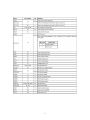
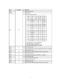
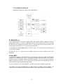
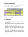
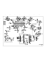
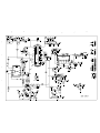
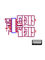
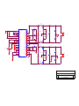
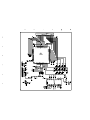
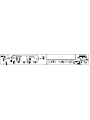
2. SYSTEM BLOCK DIAGRAM and ES6008/18 PIN DESCRIPTION
2.1 ES6008/18 PIN DESCRIPTION

5

6

7

8

9

10
2.1 SYSTEM BLOCK DIAGRAM
System block diagram is shown in the following figure:
3. AUDIO OUTPUT
The ES6008 supports two-channel analog audio output while ES6018 supports six-channel
analog audio output. In a system configuration with six analog outputs, the front left and right
channels can be configured to provide the stereo (2 channel) outputs and Dolby Surround, or the
left and right front channels for a 5.1 channel surround system.
The ES6008 also provides digital output in S/PDIF format. The board supports both optical and
coaxial S/PDIF outputs.
AV1000 Has also 5.1 channel Class-D amplifier outputs to 8 ohms satelites and 4 ohms
subwoofer.
4 AUDIO DACS
The ES6008/18 supports several variations of an I
2
S type bus, varying the order of the data bits
(leading or no leading zero bit, left or right alignment within frame, and MSB or LSB first) is
possible using the ES6008/18 internal configuration registers. The I
2
S format uses four stereo
data lines and three clock lines. The I
2
S data and clock lines can be connected directly to one or
more audio DAC to generate analog audio output.
The two-channel DAC is an AKM AK4382A. The DACs support up to 192kHz sampling rate.
The outputs of the DACs are differential, not single ended so a buffering circuit is required. The
buffer circuits use National LM833 op-amps to perform the low-pass filtering and the buffering.

11
5 VIDEO INTERFACE
5.1 Video Display Output
The video output section controls the transfer of video frames stored in memory to the internal TV
encoder of the Vibratto. The output section consists of a programmable CRT controller capable of
operating either in Master or Slave mode.
The video output section features internal line buffers which allow the outgoing luminance and
chrominance data to match the internal clock rates with external pixel clock rates, easily
facilitating YUV4: 2:2 to YUV4: 2:0 component and sample conversion. A polyphase filter
achieves arbitrary horizontal decimation and interpolation.
Video Bus
The video bus has 8 YUV data pins that transfer luminance and chrominance (YUV) pixels in
CCIR601 pixel format (4:2:2). In this format, there are half as many chrominance (U or V) pixels
per line as luminance (Y) pixels; there are as many chrominance lines as luminance.
Video Post-Processing
The Vibratto video post-processing circuitry provides support for the color conversion, scaling,
and filtering functions through a combination of special hardware and software. Horizontal up-
sampling and filtering is done with a programmable, 7-tap polyphase filter bank for accurate
non-integer interpolations. Vertical scaling is achieved by repeating and dropping lines in
accordance with the applicable scaling ratio.
Video Timing
The video bus can be clocked either by double pixel clock and clock qualifier or by a single pixel
clock. The double clock typically is used for TV displays, the single for computer displays.
Video Interface Registers
VID_SCN_HSTART
The write-only Video Screen Horizontal Start Address register contains the 13-bit horizontal pixel
starting address of the active video display.
VID_SCN_HEND
The write-only Video Screen Horizontal End Address register contains the 13-bit horizontal pixel
ending address of the active video display.
VID_SCN_VSTART
The write-only Video Screen Vertical Start Address register contains the 13-bit vertical scan line
starting address of the active video display.
VID_SCN_VEND
The write-only Video Screen Vertical End Address register contains the 13-bit vertical scan line
ending address of the active video display.
VID_SCN_VERTIRQ
The write-only Video Screen Vertical Line Interrupt register is selectable by software and contains
the line in which a vertical interrupt will occur. Line 0 is the top of the screen, as defined by the
leading edge of the VSYNC pin. Typically, an interrupt is set either just before or just after the
active video display.
VID_SCN_HBLANK_START
The write-only Video Screen Horizontal Blanking Interval Start Address register contains the 13-
bit starting address of the horizontal blanking interval for the active video display.

12
VID_SCN_HBLANK_STOP
The write-only Video Screen Horizontal Blanking Interval End Address register contains the 13-bit
ending address of the horizontal blanking stop interval for the active video display.
VID_SCN_VBLANK_START
The Video Screen Vertical Blanking Interval Start Address register contains the 13-bit starting
address of the vertical blanking interval for the active video display.
VID_SCN_VBLANK_STOP
The write-only Video Screen Vertical Blanking Interval Stop Address register contains the 13-bit
ending address of the vertical blanking stop interval for the active video display.
VID_SCN_HSYNCWIDTH
The write-only Video Screen Horizontal Sync Width Pulse register contains the 13-bit value of the
horizontal sync pulse width for the active video display. This register is needed only if sync
direction is output
VID_SCN_HSYNCPERIOD
The write-only Video Screen Horizontal Sync Period register contains the 13-bit value for the
period of the horizontal sync pulse used by the active video display. It is needed only if sync
direction is output.
VID_SCN_VSYNCPERIOD
The write-only Video Screen Video Sync Period register contains the 13-bit value for the period of
the vertical sync pulse used by the active video display. This register is needed only if sync
direction is output.
VID_SCN_VSYNCPIXEL
The write-only Video Screen Vertical Sync Pixel register defines which pixel VSYNC will change
on for the active video display. The number of pixels delayed from HSYNC that VSYNC will
change on either the rising or falling edge of VSYNC. This register is needed only if sync direction
is output
VID_SCN_VSYNCWIDTH
The write-only Video Screen Vertical Sync Pulse Width register defines the width of the 6-bit
vertical sync pulse. It is needed only if sync direction is output
VID_SCN_VERTCOUNT
The read-only Video Screen Verital Counter register contains the current line of the vertical
counter, and starts its counting at VSYNC line 0. This register is typically used for testing only.
VID_SCN_HORIZCOUNT
The read-only Video Screen Horizontal Counter register contains the current pixel of the
horizontal counter, and starts its counting at HSYNC pixel 0. This register is typically used for
testing only.
VID_SCN_COUNTER_CTL
The write-only Video Screen Counter Control register contains counter control bits for the inverted
blank sync, inverted horizontal sync, and inverted vertical sync functions. This register initializes
to 0x00 after reset.
VID_SCN_OUTPUTCNTL
The Video Screen Output Control register contains the control logic used to control the clamping
and filtering characteristics of the signal being output to the video display.

13
VID_SCN_ITERFACECNTL
The Video Screen Interface Control register contains the control logic used to determine the
signal output characteristics to the video display.
VID_SCN_RESETS
The Video Screen Reset register contains the control logic for reset events, including the reset
pan and scan, horizontal filtering and DMA enabling functions. This register is set to 1 on reset.
VID_SCN_STATUS
The Video Screen Status register contains the status bits for the video section.
VID_SCN_OSD_HSTART
The OSD Video Screen Horizontal Start Address register contains the horizontal starting address
value for the OSD, as referenced from the active display window.
VID_SCN_OSD_HEND
The OSD Video Screen Horizontal End Address register contains the 13-bit horizontal ending
address value for the OSD, as referenced from the active video display.
VID_SCN_OSD_VSTART
The OSD Video Screen Vertical Start Address register contains the 13-bit vertical starting
address value for the OSD, as referenced from the active video display.
VID_SCN_OSD_VEND
The OSD Video Screen Vertical End Address register contains the 13-bit vertical ending address
value for the OSD, as referenced from the active video display.
VID_SCN_OSD_MISC
The OSD Video Screen Miscellaneous register contains the control logic and status bits for the
OSD controller.
VID_SCN_OSD_PALETTE
These 16 registers contain the OSD palette.
6 SDRAM MEMORY
The memory bus interface generates all the control signals to interface with external memory.
The Vibratto supports different configurations using the memory configuration bits SDCFG[1:0]
(bits 12:11), the SD8BIT bit (bit 14), and SD64M bit (bit 15) in the BUSCON_DRAM_CONTROL
register. Configurations can be implemented in many ways. The following table lists the typical
SDRAM configurations used by the Vibratto.

14
Typical SDRAM Configurations:
The memory interface controls access to both external SDRAM or EDO memories, which can be
the sole unified external read/write memory acting as program and data memory as well as
various decoding and display buffers. At high clock speeds, the Vibratto memory bus interface
has sufficient bandwidth to support the decoding and displaying of CCIR601 resolution images at
full frame rate.
7 FLASH MEMORY
The decoder board supports AMD class Flash memories. Currently 4 configurations are
supported:
FLASH_512K_8b
FLASH_1024K_8b
FLASH_512Kx2_8b
FLASH_512Kx2_16b
The Vibratto permits both 8- and 16-bit common memory I/O accesses with a removable storage
card via the host interface.
8 SERIAL EEPROM MEMORY
An I2C serial EEPROM is used to store user configuration (i.e. language preferences,
speaker setup, etc.) and software configuration.. Industry standard EEPROM range in size from
1kbit to 256kbit and share the same IC footprint and pinout. The default device is 2kbit, 256kx 8,
SOIC8 SGS Thomson ST24C02M1 or equivalent.

15
9 ATA/IDE LOADER INTERFACE
The host interface can directly support ATAPI devices such as DVD drives or I/O
controllers. PIO modes 0 through 4 are supported. The ATA/IDE interface can directly control two
devices through the use of the HCS1FX# and HCS3FX# signals. The ATA/IDE interface of the
Vibratto uses a command execution protocol that allows the operation of audio-CD and DVD
loaders to coexist on the same type of interface cable that most computers use for CD loaders
and hard disk drives.
Note: The decoder board supports the standard ATAPI electrical connections, but the
software protocol within the drive is not always supported according to ATAPI specifications.
Custom software may need to be developed and tested to support ATAPI drives from different
manufacturers.
10 AUDIO INTERFACE AUDIO SAMPLING RATE AND PLL COMPONENT
CONFIGURATION
The ES6008/18 Vibratto audio mode configuration is selectable, allowing it to interface
directly with low-cost audio DACs and ADCs. The audio port provides a standard I
2
S interface
input and output and S/PDIF (IEC958) audio output. Stereo mode is in I
2
S format while six
channels Dolby Digital (5.1 channel) audio output can be channeled through the S/PDIF. The
S/PDIF interface consists of a bi-phase mark encoder, which has low skew. The transmit I
2
S
interface supports the 128, 192, 256, 384, and 512 sampling frequency formats, where sampling
frequency Fs is usually 32 kHz, 44.1 kHz, 48 kHz, 96 kHz, or 192 kHz. The audio samples for the
I
2
S transmit interface can be 16, 18, 20, 24, and 32-bit samples.
For Linear PCM audio stream format, the Vibratto supports 48 kHz and 96 kHz. Dolby
Digital audio only supports 48 kHz. The ES6008/18 Vibratto incorporates a built-in programmable
analog PLL in the device architecture in order to generate a master audio clock. The MCLK pin is
for the audio DAC clock and can either be an output from or an input to the ES6008/18 Vibratto.
Audio data out (TSD) and audio frame sync (TWS) are clocked out of the Vibratto based on the
audio transmit bit clock (TBCK). Audio receive bit clock (RBCK) is used to clock in audio data in
(RSD) and audio receive frame sync (RWS).
11 FRONT PANEL
11.1 VFD CONTROLLER
The VFD controller is a NEC uPD16311. This controller is not a processor, but does
include a simple state machine which scans the VFD and reads the front panel button matrix. The
16311 also includes RAM so it can store the current state of all the VFD icons and segments.
Therefore, the 16311 need only be accessed when the VFD status changes and when the button
status is read. The ES6008/ES6018 can control this chip directly using PIO pins or can allow the
front panel PIC to control the VFD.
12 MISCELLANEOUS FUNCTIONS
12.1 RESET CIRCUITRY
Two different chips are supported to provide the power-on-reset DS1811 or AAT3520.
12.2 VOLTAGE REGULATORS

16
There are 7812, 7805 and LM317 linear regulator ICs on the power supply to generate
+5V, -5V, +12V, -12V and +3.3V for the device. On the standby mode just +12Vst and +5V
supplies are generating for standby power consumption.
The ES6008/18 requires 2.5V to operate. This voltage is generated from +5V.
13 CONNECTORS
13.1 ATAPI DRIVE STANDARD CONNECTOR
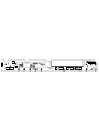
The I/O connector is a 40-pin connector as shown in figure A.1, with pin assignments as shown in table
A.1. The connector shall be keyed to prevent the possibility of installing it upside down. A key is provided
by the removal of pin 20. The corresponding pin on the cable connector shall be plugged.
The cable plug, not the receptacle, governs the pin locations. The way in which the receptacle is mounted
on the printed circuit board affects the pin positions, and pin 1 shall remain in the same relative position.
This means the pin numbers of the receptacle may not reflect the conductor number of the plug. The
header receptacle is not polarized, and all the signals are relative to pin 20, which is keyed.
By using the plug positions as primary, a straight cable can connect devices. As shown in figure A.1,
conductor 1 on pin 1 of the plug shall be in the same relative position no matter what the receptacle
numbering looks like. If receptacle numbering was followed, the cable would have to twist 180 degrees
between a device with top-mounted receptacles, and a device with bottom-mounted receptacles.
1
40 20 2
Circuit board Circuit board
1
40 20 2
Figure A.1 - 40-pin connector mounting

17
Table A.1 - 40-pin connector interface signals
Signal name Connector
contact
Conductor Connector
contact
Signal name
RESET- 1 1 2 2 Ground
DD7 3 3 4 4 DD8
DD6 5 5 6 6 DD9
DD5 7 7 8 8 DD10
DD4 9 9 10 10 DD11
DD3 11 11 12 12 DD12
DD2 13 13 14 14 DD13
DD1 15 15 16 16 DD14
DD0 17 17 18 18 DD15
Ground 19 19 20 20 (keypin)
DMARQ 21 21 22 22 Ground
DIOW- 23 23 24 24 Ground
DIOR- 25 25 26 26 Ground
IORDY 27 27 28 28 CSEL
DMACK- 29 29 30 30 Ground
INTRQ 31 31 32 32 reserved
DA1 33 33 34 34 PDIAG-
DA0 35 35 36 36 DA2
CS0- 37 37 38 38 CS1-
DASP- 39 39 40 40 Ground
Recommended part numbers for the mating connector and cable are shown below, but equivalent parts may
be used.
Connector (40 pin) 3M 3417-7000 or equivalent
Strain relief 3M 3448-2040 or equivalent
Flat cable (stranded 28 AWG) 3M 3365-40 or equivalent
Flat cable (stranded 28 AWG) 3M 3517-40 (shielded) or equivalent
13.2 SCART CONNECTORS
Pinout of the scart connector:
1 à Audio Right Out
2 à Audio Right In
3 à Audio Left / Monu Out
4 à Audio Gnd
5 à Blue Gnd
6 à Audio Left / Mono In
7 à Blue
8 à Control Voltage
9 à Green Gnd
10 à Comms Data 2

18
11 à Green
12 à Comms Data 1
13 à Red Gnd
14 à Comms Data Gnd
15 à Red
16 à Fast Blanking
17 à Video Gnd
18 à Fast Blanking Gnd
19 à Composite Video In
20 à Composite Video Out
21 à Shield
Some cheaper SCART cables use unshielded wires, which is just about acceptable for
short cable lengths. For longer lengths, shielded co-ax cable become essential.
Scart Signals:
Audio signals
0.5V RMS, <1K output impedance, >10K input impedance.
Red, Green, Blue
0.7Vpp ±2dB, 75R input and output impedance. Note that the Red connection (pin 20) can
alternatively carry the S-VHS Chrominance signal, which is 0.3V.
Composite Video / CSync
1Vpp including sync, ±2dB, 75R input and output impedance.Bandwidth = 25Hz to 4.8MHz for
normal TV Video de-emphasis to CCIR 405.1 (625-line TV)
Fast Blanking
75R input and output impedance. This control voltage allows devices to over-ride the composite
video input with RGB inputs, for example when inserting closed caption text. It is called fast
because this can be done at the same speeds as other video signals, which is why it requires the
same 75R impedances.
0 to 0.4V: TV is driven by the composite video input signal (pin 19).
Left unconnected, it is pulled to 0V by its 75R termination.
1V to 3V: the TV is driven by the signals Red, Green, Blue and composite sync. The
latter is sent to the TV on pin 19. This signal is useful when using a TV to display the
RGB output of devices such as home computers with TV-compatible frame rates. Tying
the signal to 5V via 100R forms a potential divider with the 75R termination, holding the
signal at around 2V. Alternatively, if a TTL level (0 to 5V) negative sync pulse is
available, this will be high during the display periods, so this can drive the blanking signal
via a suitable resistor.
Control Voltage
0 to 2V = TV, Normal.
5 to 8V = TV wide screen
9.5 to 12V = AV mode

19
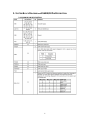
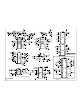
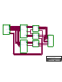
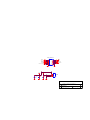
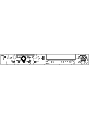
IC500 8051 Micro Controller's Main Functions:
There are 2 main functions of the IC500 8051 micro controller; signal switching and
standby controlls. IC500 communicates with ES80X6 microcontroller by using I
2
C bus. (AUX0,
AUX1 signals)
Multiplexer (MUX) control signals for signal switching supplied by IC500. These MUX
signals are using the select signal sources and input-output signals.
MUX Control Signal list is shown in the following figure:
14. CIRCUIT DESCRIPTION
14.1 POWER SUPPLY:
• Socket PL800 is the 220VAC input.
• 3.5A fuse F800 is used to protect the device against short circuit and
unexpected overloads.
• Line filter and capacitors L800, C800 and C803 are used to block the parasitic
coming from the mains. They also prevent the noise, produced in the circuit,
from being injected to the line.
• Voltage is rectified by using diodes D805 diode bridge. Using capacitor C815
(220µf) a DC voltage is produced. (310- 320VDC).
• The current in the primary side of the transformer TR800 comes to the SMPS
IC (IC800 MC44608). The SMPS IC has a eight-pin DIP-8 package and an
external MOSFET with a cooler is mounted on it. It has a built-in oscillator,
overcurrent and overvoltage protection circuitry and runs at 100kHz. It starts
with the current from the primary side of the transformer and follows the
current from the feedback winding.
• Feedback current is deteceted by optocoupler IC803. Depending on the
control current coming from the secondary side, SMPS IC keeps the output
voltage constant by controlling the duty cycle of the ~30kHz signal (PWM) at
the primary side of the transformer.

20
• Voltages on the secondary side are as follows: +20 Volts at D811, +10 Volts
at D808, +14V at D810, -22 Volts at D812, +12Vst at Q804.
• Using the output of the D808, a photo diode inside of the IC803 generates
feedback signal bu using optocoupler's photo transistor. This photo transistor
adjusts the control voltage at the IC800 pin3. The voltage at this pin effects
the pwm output frequency on the IC800 pin5. And finally output voltages
reach their correct values by this way.
• Voltage regulator IC805 (LM7805) supplies +5 Volts,
IC807 supplies +5V (off on standby mode),
IC809 supplies +3.3V (by using output of the IC807, off on standby mode),
Q804 supplies +12Vst,
IC806 supplies +12V (off on standby mode),
Q808 supplies -5V,
D812 supplies -22V.
Standby mode controlled by standby control transistors Q805, Q806, Q807.
Standby control signal comes from PL805 connector and generated by 8051
micro controllers.
• –22 Volts is used to feed the VFD (Vacuum Fluorescent Display) driver IC on
the front panel. Using diode R844, –22V is decreased and connected to the
filament winding to produce the DC offset for the filaments.
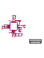
14.2 FRONT PANEL:
• All the functions on the front panel are controlled by IC1 (ES6008/18) on the
mainboard. Key scanning and IR checking operations on the standby mode
are controlled by IC500.
• ES60X8 IC sends the commands to IC1 uPD16311 via socket PL1 (pins 2,3
and 4).
• There are 16 keys scanning function, 2 LED outputs, 1 Stand-by output and
VFD drivers on IC2.
• Pin 52 is the oscillator pin and is connected via R5 56K.
• LED D5 is bright red in stand-by mode and soft red when the device is on.
• Vacuum fluorescent display MD1 is specially designed for AV1000.
• The scanned keys are transmitted via IC3 to IC1 on the mainboard.
• IR remote control receiver module IC2 (TSOP1836) sends the commands
from the remote control directly to IC1 and IC500.
• Socket PL2 carries the VFD filament voltage and –22 Volts.
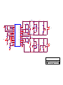
14.3 I/Os and Back Panel:
• PL303 connector on the main board carries digital audio and command
signals to Class-D amplifier board (DDX Board). Command signals are
carried by an I
2
C bus and digital audio signals are carried by I
2
S bus
interface. After processing and amplification of audio signals amplificated
audio signals comes to back panel with this order(left to right): Front Left,
Front Right, Rear Right, Center, Rear Left and Subwoofer.
La page est en cours de chargement...
La page est en cours de chargement...
La page est en cours de chargement...
La page est en cours de chargement...
La page est en cours de chargement...
La page est en cours de chargement...
La page est en cours de chargement...
La page est en cours de chargement...
La page est en cours de chargement...
La page est en cours de chargement...
La page est en cours de chargement...
La page est en cours de chargement...
La page est en cours de chargement...
La page est en cours de chargement...
La page est en cours de chargement...
La page est en cours de chargement...
La page est en cours de chargement...
La page est en cours de chargement...
La page est en cours de chargement...
La page est en cours de chargement...
La page est en cours de chargement...
La page est en cours de chargement...
La page est en cours de chargement...
La page est en cours de chargement...
La page est en cours de chargement...
La page est en cours de chargement...
La page est en cours de chargement...
La page est en cours de chargement...
La page est en cours de chargement...
La page est en cours de chargement...
La page est en cours de chargement...
La page est en cours de chargement...
La page est en cours de chargement...
La page est en cours de chargement...
-
 1
1
-
 2
2
-
 3
3
-
 4
4
-
 5
5
-
 6
6
-
 7
7
-
 8
8
-
 9
9
-
 10
10
-
 11
11
-
 12
12
-
 13
13
-
 14
14
-
 15
15
-
 16
16
-
 17
17
-
 18
18
-
 19
19
-
 20
20
-
 21
21
-
 22
22
-
 23
23
-
 24
24
-
 25
25
-
 26
26
-
 27
27
-
 28
28
-
 29
29
-
 30
30
-
 31
31
-
 32
32
-
 33
33
-
 34
34
-
 35
35
-
 36
36
-
 37
37
-
 38
38
-
 39
39
-
 40
40
-
 41
41
-
 42
42
-
 43
43
-
 44
44
-
 45
45
-
 46
46
-
 47
47
-
 48
48
-
 49
49
-
 50
50
-
 51
51
-
 52
52
-
 53
53
-
 54
54


Hitachi HTDK170E Manuel utilisateur
- Taper
- Manuel utilisateur
- Ce manuel convient également à
dans d''autres langues
- English: Hitachi HTDK170E User manual
Documents connexes
Autres documents
-
Compaq NSZ2107STTUW Manuel utilisateur
-
Matrox Multi-Channel spécification
-
NEC XT4100 Le manuel du propriétaire
-
-
-
Matrox Millennium P650 Manuel utilisateur
-
-
Motorola TRN6125A Manuel utilisateur
-
FiiO K5 Manuel utilisateur