
1
SERVICE MANUAL
US Model
Canadian Model
AEP Model
UK Model
E Model
XM-SD22X
STEREO POWER AMPLIFIER
Other Specifications
Circuit system OTL (output transformerless) circuit
Pulse power supply
Inputs RCA pin jacks
High level input connector
Outputs Speaker terminals
Through out pin jacks
Suitable speaker impedance
2 – 8 Ω (stereo)
4 – 8 Ω (when used as a bridging amplifier)
Maximum outputs 400 W × 2 (at 4 Ω)
600 W × 2 (at 2 Ω)
1,200 W (BTL, at 4 Ω)
Rated outputs (supply voltage at 14.4 V)
200 W RMS × 2 (20 Hz – 20 kHz,
0.1% THD + N, at 4 Ω)
250 W RMS × 2 (20 Hz – 20 kHz,
0.15% THD + N, at 2 Ω)
500 W RMS (BTL) (20 Hz – 20 kHz,
0.15% THD + N, at 4 Ω)
SN Ratio 93 dBA (Reference 1W into 4 Ω)
Frequency response 5 Hz – 50 kHz ( dB)
Input level adjustment range
0.3 – 6.0 V (RCA pin jacks)
1.2 – 12.0 V (High level input)
Low-pass filter 50 – 300 Hz, –12 dB/oct
Low boost 0 – 10 dB (40 Hz)
Power requirements 12 V DC car battery
(negative ground)
Power supply voltage 10.5 – 16 V
Current drain at rated output : 48 A (at 4 Ω)
Remote input : 1 mA
Dimensions Approx. 403 × 55 × 277 mm
(15
7/8 × 2 1/4 × 11 in.)
(w/h/d) not incl. projecting parts and controls
Mass Approx. 5 kg (11 lb. 1 oz.) not incl. accessories
Supplied accessories Mounting screws (4)
High level input cord (1)
Protection cap (1)
Design and specifications are subject to change without
notice.
SPECIFICATIONS
AUDIO POWER SPECIFICATIONS (US MODEL)
POWER OUTPUT AND TOTAL HARMONIC DISTORTION
200 watts per channel minimum continuous average power into
4 ohms, both channels driven from 20 Hz to 20 kHz with no more
than 0.1% total harmonic distortion per Car Audio Ad Hoc
Committee standards.
+0
–3
Ver. 1.0 2004.12
9-879-367-01
2004L04-1
© 2004.12
Sony Corporation
e Vehicle Company
Published by Sony Engineering Corporation

2
TABLE OF CONTENTS
1. GENERAL
Location and Function of Controls.......................................... 3
Connections ............................................................................. 4
2. DISASSEMBLY
2-1. Bottom Plate........................................................................ 7
2-2. Main Board Section ............................................................ 8
2-3. Main Board ......................................................................... 8
2-4. LED Board .......................................................................... 9
3. ELECTRICAL ADJUSTMENT.................................... 10
4. DIAGRAMS
4-1. Block Diagram .................................................................. 11
4-2. Schematic Diagram –Main Section (1/2)– ........................ 12
4-3. Schematic Diagram –Main Section (2/2)– ........................ 13
4-4. Printed Wiring Boards –Main Section– ............................ 14
5. EXPLODED VIEWS
5-1. Heat Sink (Main) Section.................................................. 16
5-2. Main Board Section .......................................................... 17
6. ELECTRICAL PARTS LIST......................................... 18
Notes on Chip Component Replacement
• Never reuse a disconnected chip component.
• Notice that the minus side of a tantalum capacitor may be dam-
aged by heat.
SAFETY-RELATED COMPONENT WARNING!!
COMPONENTS IDENTIFIED BY MARK 0 OR DOTTED LINE
WITH MARK 0 ON THE SCHEMATIC DIAGRAMS AND IN
THE PARTS LIST ARE CRITICAL TO SAFE OPERATION.
REPLACE THESE COMPONENTS WITH SONY PARTS WHOSE
PART NUMBERS APPEAR AS SHOWN IN THIS MANUAL OR
IN SUPPLEMENTS PUBLISHED BY SONY.
ATTENTION AU COMPOSANT AYANT RAPPORT
À LA SÉCURITÉ!!
LES COMPOSANTS IDENTIFIÉS PAR UNE MARQUE 0 SUR LES
DIAGRAMMES SCHÉMATIQUES ET LA LISTE DES PIÈCES
SONT CRITIQUES POUR LA SÉCURITÉ DE FONCTIONNEMENT.
NE REMPLACER CES COMPOSANTS QUE PAR DES PIÈCES
SONY DONT LES NUMÉROS SONT DONNÉS DANS CE MANUEL
OU DANS LES SUPPLÉMENTS PUBLIÉS PAR SONY.
XM-SD22X
Note for Replacement of FET
Change the both channels of FETs at the output stage.
If one or both parts in the following combination is broken, the
service kit should be ordered.
Service kit part No.
Q108, 110, 112
X-3383-027-1
Q208, 210, 212
Q109, 111, 113
X-3383-028-1
Q209, 211, 213

3
XM-SD22X
SECTION 1
GENERAL
This section is extracted
from instruction manual.
Features
•Maximum power output of 400 W per channel
(at 4 Ω).
• This unit can be used as a bridging amplifier
with a maximum output of 1,200 W.
•Direct connection can be made with the speaker
output of your car audio unit if it is not equipped
with a line output (High level input connection).
• Built-in variable LPF (Low-pass filter) and low
boost circuit.
• Dual mode connection possible for a multi-
speaker system.
• Protection circuit.
• Pulse power supply * for stable, regulated output
power.
*
Pulse power supply
This unit has a built-in power regulator which
converts the power supplied by the DC 12 V car
battery into high speed pulses using a
semiconductor switch. These pulses are stepped
up by the built-in pulse transformer and
separated into both positive and negative power
supplies before being converted into direct
current again. This light weight power supply
system provides a highly efficient power supply
with a low impedance output.
Caractéristiques
• Puissance de sortie maximale de 400 W par canal
(à 4 Ω).
• Cet appareil peut être utilisé comme
amplificateur en pont d’une sortie maximale de
1 200 W.
• Une connexion directe est possible avec la sortie
haut-parleur de votre autoradio si celle-ci n’est
pas équipée d’une sortie de ligne (connexion
d’entrée haut niveau).
•Filtre passe-bas (LPF) intégré et circuit
d’amplification de basses fréquences.
• Double mode de connexion possible au moyen
d’un système à plusieurs haut-parleurs.
•Circuit de protection.
•Alimentation électrique par impulsions * pour
une puissance de sortie stable, régulée.
*
Alimentation électrique par impulsions
Cet appareil est équipé d’un régulateur de
puissance intégré qui convertit la puissance
fournie par une batterie de voiture de 12 V CC en
impulsions ultra-rapides au moyen d’un
commutateur à semi-conducteur. Ces impulsions
sont amplifiées par le transformateur
d’impulsions intégré et séparées en alimentation
positive et négative avant d’être reconverties en
courant continu. Ce système d’alimentation de
faible poids assure une alimentation électrique
très efficace pour une sortie d’impédance faible.
Circuit Diagram
Schéma du circuit
Low boost
Amplification de basses fréquences
Frequency/Fréquence
dB
Frequency/Fréquence
dB
Cut-off frequency (LPF)
Fréquence de coupure (LPF)
PROTECTOR
FILTER
OFF
LPF
LEVEL
LOW BOOST
(40Hz)
0 +10dB
6
0.3V
2
4
5.5
0.5
60
50 300Hz
170
110
260
10
10
0
40 100 1k
10
0
-10
-20
-30
-40
-50
-60
-70
-80
10 100 1k
50Hz
170Hz
300Hz
LEVEL
LPF
Normal
AMP
Power
Lch
LEVEL
Inverted
AMP
Power
Rch
BTL
Lch
Rch
(BTL.)
LOW BOOST
LOW BOOST
Hz
Hz
Location and Function
of Controls
1 PROTECTOR indicator
When the PROTECTOR is activated, the
indicator lights up in red.
When the PROTECTOR is activated refer to
the Troubleshooting Guide.
2 LEVEL adjustment control
The input level can be adjusted with this
control. Turn it in the clockwise direction
when the output level of the car audio unit
seems low.
3 LOW BOOST level control
Tu rn this control to boost the frequencies
around 40 Hz to a maximum of 10 dB.
4 Cut-off frequency adjustment control
Sets the cut-off frequency (50 – 300 Hz) for
the low-pass filter.
5 FILTER selector switch
When the switch is in the LPF position, the
filter is set to low-pass.
Emplacement et fonction
des commandes
1 Indicateur PROTECTOR
Lorsque PROTECTOR est activé,
l’indicateur s’allume en rouge.
Lorsque PROTECTOR est activé, reportez-
vous au guide de dépannage.
2 Commande de réglage LEVEL
Le niveau d’entrée peut se régler avec cette
commande. Tournez cette commande dans
le sens des aiguilles d’une montre lorsque le
niveau de sortie de l’autoradio semble
faible.
3 Commande de niveau LOW BOOST
Tournez cette commande pour amplifier les
fréquences autour de 40 Hz jusqu’à un
maximum de 10 dB.
4 Commandes de réglage de la fréquence
de coupure
Permet de régler la fréquence de coupure
(50 – 300 Hz) pour le filtre passe-bas.
5 Sélecteur FILTER
Lorsque le sélecteur est en position LPF, le
filtre est réglé sur passe-bas.

4
XM-SD22X
BTL BTL
OFF
LPF
BTL BTL BTL BTL
Connections
Caution
• Before making any connections, disconnect
the ground terminal of the car battery to avoid
short circuits.
• Be sure to use speakers with an adequate
power rating. If you use small capacity
speakers, they may be damaged.
• Do not connect the # terminal of the speaker
system to the car chassis, and do not connect
the # terminal of the right speaker with that
of the left speaker.
• Install the input and output cords away from
the power supply wire as running them close
together can generate some interference noise.
• This unit is a high powered amplifier.
Therefore, it may not perform to its full
potential if used with the speaker cords
supplied with the car.
• If your car is equipped with a computer
system for navigation or some other purpose,
do not remove the ground wire from the car
battery. If you disconnect the wire, the
computer memory may be erased. To avoid
short circuits when making connections,
disconnect the +12 V power supply wire until
all the other wires have been connected.
Connexions
2-Speaker System
Système à 2 haut-parleurs
Car audio unit
Autoradio
LINE OUT
Left speaker
(min. 2 Ω)
Haut-parleur
gauche
(min. 2 Ω)
Right speaker
(min. 2 Ω)
Haut-parleur
droit
(min. 2 Ω)
As a Monaural Amplifier
Comme amplificateur monaural
Car audio unit
Autoradio
LINE OUT
Right channel
Canal droit
Left channel
Canal gauche
Right speaker
(min. 4 Ω)
Haut-parleur droit
(min. 4 Ω)
Pour plus de détails sur les réglages des
commutateurs et commandes, reportez-vous à
« Emplacement et fonction des commandes ».
Remarque
Vérifiez que la sortie de ligne de l’autoradio est
raccordée à la prise portant l’indication
« L (BTL) » sur l’appareil.
Left speaker (min. 4 Ω)
Haut-parleur gauche
(min. 4 Ω)
As the Monaural Amplifier for a Subwoofer
Comme amplificateur monaural pour un haut-parleur
d’extrêmes graves
Car audio unit
Autoradio
LINE OUT
For details on the settings of switches and
controls, refer to “Location and Function of
Controls.”
Note
Make sure that the line output from the car
audio unit is connected to the jack marked
“L (BTL)” on the unit.
For details on the settings of switches and
controls, refer to “Location and Function of
Controls.”
Note
If you wish to use a subwoofer as a monaural
speaker, connect the speaker as illustrated
above. The output signals to the subwoofer
will be the combination of the both right and
left output signals.
Pour plus de détails sur les réglages des
commutateurs et commandes, reportez-vous à
« Emplacement et fonction des commandes ».
Remarque
Si vous désirez utiliser un haut-parleur
d’extrêmes graves comme haut-parleur
monaural, raccordez le haut-parleur comme
illustré ci-dessus. Les signaux de sortie vers le
haut-parleur d’extrêmes graves seront une
combinaison des signaux de sortie droit et
gauche.
Attention
• Avant d’effectuer les connexions, débranchez
la borne de masse de la batterie de voiture
pour éviter tout court-circuit.
• Veillez à utiliser des haut-parleurs de
puissance adéquate. Si vous utilisez des haut-
parleurs de faible capacité, ils risquent d’être
endommagés.
• Ne raccordez pas la borne # du système de
haut-parleurs à la carrosserie de la voiture ni
la borne # du haut-parleur droit avec celle du
haut-parleur gauche.
• Eloignez les câbles d’entrée et de sortie du
câble d’alimentation pour éviter les
interférences.
• Cet appareil est un amplificateur de haute
puissance. Il ne peut donc déployer sa pleine
puissance que si les câbles de haut-parleurs de
la voiture lui sont raccordés.
• Si votre voiture est équipée d’un système de
navigation ou d’un ordinateur de bord, ne
retirez pas le fil de terre de la batterie de la
voiture, sinon les données mémorisées seront
effacées. Pour éviter un court-circuit lorsque
vous effectuez les branchements, branchez le
câble d’alimentation +12 V après avoir
branché tous les autres fils.
Power Connection Wires
Câbles d’alimentation
Car audio unit
Autoradio
Fuse (80 A)
Fusible (80 A)
+12 V car battery
Batterie de voiture +12 V
Remote output
*
1
Sortie de
commande
*
1
(REM OUT)
to a metal point
of the car
vers une partie
métallique de la
carrosserie
*
1
If you have the factory original or some other car audio unit without a remote output for the amplifier,
connect the remote input terminal (REMOTE) to the accessory power supply.
*
1
Si vous disposez du modèle d’origine ou d’un autre autoradio sans aucune sortie de commande à
distance pour l’amplificateur, raccordez la borne d’entrée de la commande à distance (REMOTE) à la
prise d’alimentation accessoires.
Notes on the power supply
•
Connect the +12 V power supply wire only after
all the other wires have been connected.
•
Be sure to connect the ground wire of the unit
securely to a metal point of the car. A loose
connection may cause a malfunction of the
amplifier.
•
Be sure to connect the remote control wire of the
car audio unit to the remote terminal.
• When using a car audio unit without a remote
output on the amplifier, connect the remote
input terminal (REMOTE) to the accessory power
supply.
•
Use the power supply wire with a fuse attached
(80 A).
•
All power wires connected to the positive battery
post should be fused within 450 mm (18 in) of the
battery post, and before they pass through any
metal.
•
Make sure that the vehicle’s battery wires
connected to the vehicle (ground to chassis)
*
2
are
of a wire gauge at least equal to that of the main
power wire connected from the battery to the
amplifier.
•
Make sure that the wires to be connected to the
+
12 V and GND terminals of this unit are at least
4-Gauge (AWG-4) or have a sectional area of
more than 22.0 mm
2
(
7
/
8
in
2
).
Remarques sur l’alimentation électrique
•
Raccordez le câble d’alimentation +12 V
uniquement après avoir réalisé toutes les autres
connexions.
•
Raccordez correctement le fil de masse à une
partie métallique de la voiture. Une connexion
lâche peut provoquer un dysfonctionnement de
l’amplificateur.
•
Veillez à raccordez le fil de commande à distance
de l’autoradio à la borne de commande à
distance.
•
Si vous utilisez un autoradio dont l’amplificateur
ne comporte pas de sortie de commande à
distance, raccordez la borne d’entrée de la
commande à distance (REMOTE) à la prise
d’alimentation accessoires.
•
Utilisez un câble d’alimentation muni d’un fusible
(80 A).
•
Tous les fils électriques raccordés au support de
batterie positif doivent être protégés par un
fusible à une distance maximum de 450 mm (18
po) du support de batterie et avant de passer
dans une partie métallique quelconque.
•
Assurez-vous que les fils de la batterie du véhicule
raccordés à ce dernier (sol au châssis)
*
2
sont d’un
calibre au moins égal à celui du fil électrique
principal reliant la batterie et l’amplificateur.
•
Assurez-vous que les câbles à raccorder aux
bornes +12V et GND de cet appareil sont d’un
calibre d’au moins 4 (AWG-4) ou d’une section
supérieure à 22,0 mm
2
(
7
/
8
po
2
).
Pour plus de détails sur les réglages des
commutateurs et commandes, reportez-
vous à « Emplacement et fonction des
commandes ».
For details on the settings of switches and
controls, refer to “Location and Function of
Controls.”
Subwoofer (min. 4 Ω)
Haut-parleur d’extrêmes
graves (min. 4 Ω)
Make the terminal connections as illustrated below.
Procédez aux connexions des bornes comme illustré ci-dessous.
R
E
M
+
1
2
V
G
N
D
REM
+
12V GND
Pass the wires through the cap, connect
the wires, then cover the terminals with
the cap.
Note
When you tighten the screw, be careful not to
apply too much torque
*
as doing so may damage
the screw.
*
The torque value should be less than 1 N•m.
Faites passer les fils par le cache, raccordez
les fils, puis recouvrez les bornes avec le
cache.
Remarque
Lorsque vous vissez la vis, faites attention à ne
pas appliquer une trop grande force
*
, car cela
pourrait l’endommager.
*
Le couple de torsion doit être inférieur à 1 N•m.
3
3
c
less than 450 mm (18 in)
moins de 450 mm (18 po)
*
2

5
XM-SD22X
BTL BTL
OFF
LPF
OFF
LPF
OFF
LPF
OFF
LPF
OFF
LPF
Four output channels
Quatre canaux de sortie
Full range speakers
(min. 2 Ω)
Haut-parleurs à
gamme étendue
(min. 2 Ω)
Subwoofers (min. 2 Ω)
Haut-parleur d’extrêmes
graves (min. 2 Ω)
Pour plus de détails sur les réglages des
commutateurs et commandes, reportez-vous à
« Emplacement et fonction des commandes ».
Remarque
Dans ce système, le volume des haut-parleurs
d’extrêmes graves est contrôlé par la commande
de balance avant/arrière de l’autoradio.
For details on the settings of switches and
controls, refer to “Location and Function of
Controls.”
Note
In this system, the volume of the subwoofers
will be controlled by the car audio unit fader
control.
Car audio unit
Autoradio
LINE OUT
Dual Mode System (With a Bridged Subwoofer)
Double mode de connexion (avec un haut-parleur
d’extrêmes graves en pont)
Notes
• When using passive crossover networks in a multi-
speaker system, care must be taken as the speaker
system’s impedance should not be lower than that
of the suitable impedance for this unit.
• When you are installing a 12 decibels/octave system
in your car, the following points must be
considered. In a 12 decibels/octave system where
both a choke and capacitor are used in series to
form a circuit, a great care must be taken when
they are connected. In such a circuit, there is going
to be an increase in the current which by-passes the
speaker with frequencies at around the crossover
frequency. If audio signals are continued to be fed
into the crossover frequency area, it may cause the
amplifier to become abnormally hot or the fuse will
be blown. Also if the speaker is disconnected, a
series-resonant circuit will be formed by the choke
and the capacitor. In this case, the impedance in the
resonance area will decrease dramatically resulting
in a short circuit like situation causing a damage to
the amplifier. Therefore, make sure that a speaker
is connected to such a circuit at all times.
Remarques
• Lorsque vous utilisez des circuits de recoupement de
fréquence passifs dans un système à plusieurs haut-parleurs,
assurez-vous que l’impédance du système n’est pas inférieure
à celle prévue pour cet appareil.
• Lorsque vous installez un système à 12 décibels/octave dans
votre voiture, vous devez respecter les points suivants. Dans
un système à 12 décibels/octave où la bobine d’arrêt et le
condensateur sont utilisés en série pour former un circuit,
vous devez réaliser les branchements avec beaucoup de
précaution. Dans ce type de circuit, une augmentation du
courant contournant le haut-parleur se produit dans les
fréquences se situant autour de la fréquence de coupure. Si
des signaux audio continuent d’être fournis dans la zone de
la fréquence de recoupement, une surchauffe risque de se
produire dans l’amplificateur et le fusible risque de griller. Si
le haut-parleur n’est pas raccordé, un circuit de résonance
série sera créé par la bobine et le condensateur. Dans ce cas,
l’impédance dans la zone de résonance sera
considérablement réduite, et comme dans le cas d’un court-
circuit, l’amplificateur peut être endommagé. Par
conséquent, veillez à ce qu’un haut-parleur soit toujours
raccordé au circuit.
C1/C2
(capacitor)
*
unit: µF
800
500
400
300
270
200
150
100
68
50
39
Table of crossover values for 6 dB/octave
(4 Ω)
* (not supplied)
Crossover
Frequency
unit: Hz
50
80
100
130
150
200
260
400
600
800
1000
L
(coil)
*
unit: mH
12.7
8.2
6.2
4.7
4.2
3.3
2.4
1.6
1.0
0.8
0.6
Fréquence de
recoupement
unité : Hz
50
80
100
130
150
200
260
400
600
800
1000
L
(bobine)
*
unité : mH
12,7
8,2
6,2
4,7
4,2
3,3
2,4
1,6
1,0
0,8
0,6
C1/C2
(condensateur)
*
unité : µF
800
500
400
300
270
200
150
100
68
50
39
Tableau des valeurs de recoupement
pour 6 dB/octave (4 Ω)
* (non fournis)
2-way System
Système 2 voies
Two output channels
Deux canaux de sortie
Full range speakers
(min. 2 Ω)
Haut-parleurs à
gamme étendue
(min. 2 Ω)
Subwoofers (min. 2 Ω)
Haut-parleurs d’extrêmes
graves (min. 2 Ω)
Car audio unit
Autoradio
LINE OUT
THROUGH OUT
INPUT
INPUT
Car audio unit
Autoradio
Left speaker
Haut-parleur gauche
Right speaker
Haut-parleur droit
Subwoofer
Haut-parleur d’extrêmes graves
LINE OUT
C2C1
L
High Level Input Connection
(As a Monaural Amplifier for a Subwoofer)
Connexion d’entrée à haut niveau
(Comme amplificateur monaural pour un haut-parleur d’extrêmes graves)
Pour plus de détails sur les réglages des
commutateurs et commandes, reportez-vous à
« Emplacement et fonction des commandes ».
Remarque
Si vous désirez utiliser un haut-parleur d’extrêmes
graves comme haut-parleur monaural, raccordez
le haut-parleur comme illustré ci-dessus. Les
signaux de sortie vers le haut-parleur d’extrêmes
graves seront une combinaison des signaux de
sortie droit et gauche.
For details on the settings of switches and
controls, refer to “Location and Function of
Controls.”
Note
If you wish to use a subwoofer as a monaural
speaker, connect the speaker as illustrated
above. The output signals to the subwoofer
will be the combination of both right and left
output signals.
Car audio unit
Autoradio
Left speaker
Haut-parleur gauche
Right speaker
Haut-parleur droit
Subwoofer (min. 4 Ω)
Haut-parleur d’extrêmes
graves (min. 4 Ω)
2
*
Lorsque vous raccordez des amplificateurs à
l’aide des prises à broches THROUGH OUT, vous
pouvez raccorder jusqu’à trois amplificateurs.
Sinon les niveaux de sortie requis ne peuvent
pas être obtenus et votre auto-radio risque
d’être endommagé.
Utilisez la borne THROUGH OUT lorsque vous
installez plusieurs amplificateurs. Les signaux
audio transitent par les prises à broches
THROUGH OUT sans subir aucun traitement.
When you connect amplifiers using the
THROUGH OUT pin jacks, it allows you to
connect up to a maximum of three.
Otherwise the necessary output levels can not
be obtained, and your car audio unit may be
damaged.
Use the THROUGH OUT terminal when you
install more amplifiers. Audio signals pass
through the THROUGH OUT pin jacks
unaffected by any signal processing.

6
XM-SD22X
BTL BTL BTL BTL
* High Level Input Connector
* Connecteur d’entrée à haut niveau
High Level Input Connection
(As a Monaural Amplifier)
Connexion d’entrée à haut niveau
(Comme amplificateur monaural)
Pour plus de détails sur les réglages des
commutateurs et commandes, reportez-vous à
« Emplacement et fonction des commandes ».
For details on the settings of switches and
controls, refer to “Location and Function of
Controls.”
Car audio unit
Autoradio
Right speaker output
Sortie haut-parleur
droit
Left speaker output
Sortie haut-parleur gauche
Left speaker
(min. 4 Ω)
Haut-parleur gauche
(min. 4 Ω)
Right speaker
(min. 4 Ω)
Haut-parleur droit
(min. 4 Ω)
Black-striped cord
Cordon rayé noir
Black-striped cord
Cordon rayé noir
Black-striped cord
Cordon rayé noir
High Level Input Connection
(2-Speaker System)
Connexion d’entrée à haut niveau
(Système à 2 haut-parleurs)
Left speaker
(min. 2 Ω)
Haut-parleur gauche
(min. 2 Ω)
Right speaker
(min. 2 Ω)
Haut-parleur droit
(min. 2 Ω)
Grey
Gris
White
Blanc
Car audio unit
Autoradio
Pour plus de détails sur les réglages des
commutateurs et commandes, reportez-vous à
« Emplacement et fonction des commandes ».
For details on the settings of switches and
controls, refer to “Location and Function of
Controls.”
Right speaker output
Sortie haut-parleur droit
Left speaker output
Sortie haut-parleur gauche
Black-striped cord
Cordon rayé noir
Grey
Gris
Grey/Black striped
Gris/Rayé noir
White
Blanc
White/Black striped
Blanc/Rayé noir
2
*
2
**
2
Black-striped cord
Cordon rayé noir
Black-striped cord
Cordon rayé noir

7
XM-SD22X
SECTION 2
DISASSEMBLY
Note : Follow the disassembly procedure in the numerical order given.
2-1. BOTTOM PLATE
Note : This set can be disassemble according to the following sequence.
2-1. BOTTOM PLATE
(Page 7)
2-2. MAIN BOARD SECTION
(Page 8)
2-4. LED BOARD
(Page 9)
SET
2-3. MAIN BOARD
(Page 8)
4
bottom plate
5
insulating shee
t
1
two screws
(+
BTP
3
x
6)
3
two screws
(+
BTP
3
x
6)
2
two screws
(+
BTP
3
x
6)

8
XM-SD22X
2-3. MAIN BOARD
2-2. MAIN BOARD SECTION
heat sink (main
)
6
CN810
5
MAIN board section
1
four screws
(+
P
3
x
8)
2
three screws
(+
P
3
x
8)
3
three screws
(+
P
3
x
8)
4
screw
(+
P
3
x
8)
3
front panel
4
MAIN board
1
two screws
(+
P
3
x
8)
2
three screws
(+
P
3
x
8)

9
XM-SD22X
2-4. LED BOARD
3
LED board
2
bracket (LED)
heat sink (main)
1
three screws
(+
P
3
x
8)

10
XM-SD22X
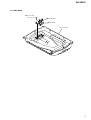
SECTION 3
ELECTRICAL ADJUSTMENT
Stabilized
Power supply
B+, REM terminal
set
GND termina
l
— MAIN BOARD (CONDUCTOR SIDE) —
RV103
BIAS ADJUSTMENT
(L-CH)
RV203
BIAS ADJUSTMEN
T
(R-CH)
Bias Adjustment
Note :In Bias Adjustment, adjust RV103 if any of Q108 through
Q113 are replaced. Adjust RV203 if any of Q208 through
Q213 are replaced.
Condition :This adjustment should be performed about one minute
after the remote mode is turned on at a room tempera-
ture of about 25°C.
Setting :
Procedure :
1. Turn the variable resistors RV103 (L-CH) and RV203 (R-CH)
full clockwise as seen from the component side to minimize the
bias current.
2. The input signal is to be no signal.
3. Apply the voltage to the B+ and REM terminals from the stabi-
lized power supply and gradually increase it up to 12.0 V while
checking for any unusual current.
4. Adjust each of RV103 (L-CH) and RV203 (R-CH) so that the
power current of the stabilized power supply is increased in steps
of 700 mA (total of 1.4 A).
5. After adjustment, check that the power current is at 1.65 to 2.05 A.
Adjustment Location : Main board (component side)

11 11
XM-SD22X
XM-SD22X
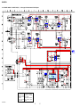
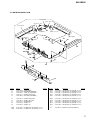
4-1. BLOCK DIAGRAM
SECTION 4
DIAGRAMS
6
5
7
3
2
1
PRE AMP
IC101 (1/2)
PRE AMP
IC102 (1/2)
3
2
L.P.F
IC301
5
6
7
LOW BOOST
IC102 (2/2)
DIFFERENTIAL
AMP
Q103
POWER
AMP
Q108,Q110,Q112
OVER CURRENT
DET
Q114
DRIVE
AMP
Q105
DIFFERENTIAL
AMP
Q104
POWER
AMP
Q109,Q111,Q113
DRIVE
AMP
Q106
BIAS
Q107
BOOST
EQUALIZER
Q101
FILTER
S801-1
OFF
LPF
RV102-1
LOW
BOOST
(40Hz)
+16.7V
(B+)
–16.7V
(B-)
CNJ801-1,-3
INPUT
OUTPUT
(THROUGH)
OUTPUT
(THROUGH)
L
(BTL)
SPEAKER OUT
L
R
LINE
SWITCH
Q102
REM
+12V
GND
PROTECTOR
3
2
10
1
3
2
1
PRE AMP
IC101 (2/2)
PRE AMP
IC202 (1/2)
5
6
7
LOW BOOST
IC202 (2/2)
DIFFERENTIAL
AMP
Q203
POWER
AMP
Q208,Q210,Q212
OVER CURRENT
DET
Q214
DRIVE
AMP
Q205
DIFFERENTIAL
AMP
Q204
POWER
ON/OFF
Q903
LINE SWITCH
CONTROL
Q701,702
POWER
AMP
Q209,Q211,Q213
DRIVE
AMP
Q206
BIAS
Q207
BOOST
EQUALIZER
Q201
RV102-2
LOW
BOOST
(40Hz)
+16.7V
(B+)
–16.7V
(B-)
CNJ801-2,-4
CNJ803
INPUT
R
L
HIGH LEVEL
INPUT
R
LINE
SWITCH
Q202
RV203
BIAS
RV103
BIAS
DC OFFSET
DET
Q802,Q803,Q804
15
16
1
2
14
12
B+
SWITCH
Q901,Q902
TEMP.DET
Q809
TH801,803,808
PTH801
DC DET
IC902
REF.
REG
PROTECT LATCH
Q801,Q805,Q806
HI-VOLTAGE
DET
IC903,Q920
CN801
F902
RECT
D911,917
RECT
D909
RECT
D905
RECT
D910
+16.7V
(B+)
+54V
(B+)
+45V
(B+)
RECT
D906
-45V
(B-)
–54V
(B–)
–16.7V
(B–)
SWITCHING
DRIVER
Q904,Q905,Q906
SWITCHING
DRIVER
Q907,Q908,Q909
DRIVER
Q910
SWITCHING
Q913
SWITCHING
Q912
11
9
8
D854
D919
D920
DC-DC
CONVERTER
TRANSFORMER
T901
DC-DC CONVERTER
IC901
D803
D820,822,827,832
+45V
(B+)
-45V
(B-)
• Signal path
: AUDIO
CN804
BTL
BTL
CN805
1
2
1
2
2
3
INV. AMP
IC302 (2/2)
5 7
L.P.F
IC302 (1/2)
RV301-1
FILTER
RV101-1
LEVEL
RV101-2
LEVEL
RV301-2
FILTER
F901
FILTER
S801-2
OFF
LPF
-1
-3
-4
-2
DRIVER
Q911
B-REG
Q915
B+REG
Q914
L
1
RECT
D912,918
1
D850,852
(POWER)
D851,853
(POWER)

12 12
XM-SD22X
XM-SD22X
IC B/D
C211
C212
TH803
TH808
PTH801
C806
R211R210
C104
R104
C109
C110
R109
RV101
R108
C103
R103
R106C108
R107
C130
R101
R102
C101
R154
C131
C231
C221
R254
C106
C105
R105
C107
C102
R206C207
R207C208
R205
C201
R202 C230
R201
C202
C209
R209
R208
C204 R204
C203R203
C205C222 C206
C210
L901
L903
C914
C915
C805
R809
R811
R810
CN810
C804
R812
R818
R903
C908
R902
R901
IC901
R938
R939
R941
R942
R940
R310
R309
C305
C304
R308
R307
R306
R305
C302
R302
RV301
C303
R120
R110 R111
C112
C111
R220
R909
R907
R913R908
R906
C911
C912
C913
R912
R911
R910
S801
R301
R820
R828 R823 R821
R833
R844
R905
C907
R904
C909
Q901
D902
CNJ801
CN803
IC302(1/2)
IC302(2/2)
RV301
S801
RV101
CN801
C902
CNJ801
IC301
TH801
R834
Q920
F902
F901
Q806
Q805
Q809
Q903
Q902
D850
D852D853
D851
D854
R853
R857
JR800
IC101(1/2)
IC101(2/2)
IC202(1/2)
IC102(1/2)
R819
R815
R835
D803
D820
IC902
IC903
D915
D901
CN852
R850R851
R856
R854
C301
R304
R303
D832
D827
D822
4-2. SCHEMATIC DIAGRAM — MAIN SECTION (1/2) — • Refer to page 15 for Waveform and IC Block Diagram.
(Page 13)
Note:
The components identi-
fied by mark 0 or dotted
line with mark 0 are criti-
cal for safety.
Replace only with part
number specified.
Note:
Les composants identifiés par
une marque 0 sont critiques
pour la sécurité.
Ne les remplacer que par une
piéce portant le numéro
spécifié.

13 13
XM-SD22X
XM-SD22X
C938
C939
C932
C933
D911
D912
D917
D918
Q908
L902
L904
RV102
R918
R928
R929R930
R931 R932
R933
R919
R144
C860
C116
R121
C118
R123
R126R125
R124
R122
C216
R223
C218
R224
C217
R222
R225 R226
R229
R702
R701
R916
R915
Q909
Q907
R917
R921
R920
R914
Q904
Q905
Q906
C920
C919
C918
C917
R803
C802
C803
R804
R806
R807
R808
R805
C225
R236
R256
R232
R234
R233
R241
C223
R230
C227
R240
C224R235
R231
RV203
R132
R136 C125
R156
R134
R129
R130
C124R135
R131
R155
RV103
C127
Q108
Q110
Q112
R801
C801
R802
R160
Q113
Q212
Q111
Q210
Q109
Q208
R247
R245
R243
R261
R260
R248
R246
R244
Q207
Q213
Q211
Q209
C904 C906
C905 C903
R860
R936
C936
R937
C937
C935
C934
C940
C941
R252
C228
R253
R153
C128
R141
C123
Q103
Q203
Q104
Q204
R255
R148
R146
R147
R145
R143
R800
Q107
R239
R133
C117
C701
C927
C928
D913
D914
C901
RV102
R221
CN804
CN805
R149
R249
T901
R238
R138
R140
R139
R161
R924
R927
C916
C921 C922 C923
C924 C925 C926
R251
R250
R151
R150
C232 C226
C132 C126
R152
Q101
Q102
Q105
Q106
D108
D106
D107
D109
D208
D206
D207
D209
Q801
Q114
Q201
Q202
Q205
Q206
Q214
Q702
R704
R703
Q701
Q803
Q802
Q910
Q911
Q912
Q913
R943
C942
C943
R944
D905
D906
L906
L905
L908
L907
Q914
Q915
Q804
D909
D910
IC102(2/2)
IC202(2/2)
D701
D702
D703
D919
D920
D204
R242
R142
D104
D801
D802
4-3. SCHEMATIC DIAGRAM — MAIN SECTION (2/2) —
(Page 12)

14 14
XM-SD22X
XM-SD22X
1
A
B
C
D
E
F
G
H
I
J
2345678910111213
TP23
TP24
JR206
JR207
JR204
JR205
FMB1
JR103
JR208
TP26
JR106
JR107
JR216
JR217
TP25
TP05
TP22
TP27
JR100
TP16
TP18
TP29
TP11
TP14
TP17
TP12
TP15
TP19
TP20
TP21
TP28
TP07
TP08
TP09
TP10
TP13
TP04
TH803
R154
R143
R144
C127
R146
R147
R130
R702
R248
R804
D915
R823
D822
C903
R807
Q914
C906
R244
R135
IC901
TH801
D207
D909 D910
D911
D918
D917
D912
R911
C913
R910
R912
Q903
Q902
R907
R908
R909
D902
D901
C908
R902
R818
R903
C806
R160
Q702
TH808
R901
R905
C941
D913
D914
R936
R937
Q915
Q214
R942
R145
R939
Q701
R703
R906
D701
R940
R811
R941
R938
R138
Q920
R844
R913
R821
D820
Q911
Q910
R246
Q114
R245
R247
R234
D208
R260
R261
R140
R161
R253
C227
D104
C940
R139
R803
R704
D702
C914
D703
R701
D803
R808
Q203Q204
R233
R124
R235
R231
R805
Q809
R802
R800
Q801
Q805
Q806
R812
R809
R810
C804
C225
R232
PTH801
Q802
C803
D919
D920
Q804
Q803
R806
R148
C224
C226
R256 R255
C927
C928
R153
R133
Q104
Q103
R134
R236
R136
R132
C124
R131
C125
C126
R155
R156
R129
R229
Q102
Q202
C904
C905
R230
R828
D827
D206
R239
R240
R833
D832
IC101
IC202
IC102
R125
R126
R225
R226
C110
R123
R107
R121
C116
R220
R207
R203
C216
R223
R221
C210
IC301
C118
R224
Q101
Q201
R209
C218
C221
C231
R254
C108
C106
C205
C206
C105
R205
R105
R109
R103
R208
R834
R120
C222
C902
C943
C901
R110
R222
IC302
R308
R108
R210
R122
R309
R310
C305
C303
R111
R211
R307
C304
C232
C132
R815
R944
R943
C942
D108
R820
D209
D106
R835
R819
R904
TP01
TP02
TP03
R915
R860
C860
R928
R929
R931
R933
Q913
R916
R917
R920
Q912
R919
R918
R921
R924
R914
R927
TP06
R930
R932
CN801
JW133
JW129
JW128
JW119
JW121
JW120
RV103
JW191
JW115
JW116
JW117
JW118
JW123
JW113
JW114
JW112
JW111
JW110
JW329
JW330
JW194
JW257
C918
C919
C917
Q907
Q908
Q909
Q906
C920
JW127
JW126
D905
JW138
C924
C925
JW145
C921
C922
JW109
C915
JW108
Q213
Q211
Q209
Q208
Q110
Q112
Q111
Q113
JW144
JW143
D906
JW136
JW134
Q904
R150
JW135
JW130
JW131
JW132
JW140
JW122
JW331
C701
C926
L901 L903
R152
Q109
Q108
R151
R149
Q210
Q212
R250 R249
R251
Q905
C916
C923
JW156
JW107
JW152
JW158
JW345
JW332
JW159
C128
JW148
JW157
Q901
JW124
JW163
C909
R141
JW105
JW104
JW106
JW243
JW199
JW149
JW147
JW146
JW150
JW137
JW141
JW142
Q207
JW171
IC902
C907
C911
JW184
R252
C228
JW187
C938
C939
C932
C933
JW181
JW179
JW174
JW180
JW241
JW178
C937
C936
C935
C934
JW151
JW189
JW188
JW264
L907
JW255
JW139
JW283
IC903
JW347
JW353
JW164
JW237
R142
Q107
JW183
JW204
JW166
JW210
JW209
JW205
JW289
JW293
JW207
JW217
JW356
JW153
JW292
JW290
JW288
JW291
JW280
JW285
JW279
JW242
JW201
JW203
JW226
JW216
JW202
JW165
L902
JW230
JW232
JW236
JW200
JW233
JW231
JW334
JW256
JW161
JW272
R242
JW125
C123
JW247
Q205
Q206
JW274
JW273
C805
JW190
JW260
JW197
JW196
R241
JW219
JW218
C223
JW234
JW169
JW235
JW182
JW198
JW220
C802
JW195
JW282
JW284
JW286
JW287
JW168
JW167
L908
L906
JW160
JW343
RV203
JW344
JW333
Q106
Q105
JW276
JW275
JW346
JW342
JW341
JW348
JW349
JW340
JW215
JW208
JW355
L905
CN805
JW258
JW206
JW277
JW278
JW170
JW259
JW154
JW352
JW175
JW246
JW245
JW248
JW249
JW261
JW262
JW263
JW281
JW186
CNJ801
RV102
RV301
JW185
C101
C109
C209
C211
C202
C201
C131
C102
C111
C212
C112
JW301
S801
JW296
JW173
JW297
JW294
JW300
C217
C117
JW312
JW303
JW326
JW328
JW354
JW311
JW295
JW316
JW313
C912
RV101
JW327
JW299
JW302
JW305
JW321
JW162
JW320
JW306
JW323
JW319
JW350
JW322
JW307
JW308
JW310
JW317
JW318
JW324
JW314
JW315
JW309
JW304
JW325
JW298
CN804
L904
CN803
JW172
D109
D107
JW240
JW239
JW238
C107
C208
C207
R102
R101
R104
R106
C103
C130
C104
C302
C301
R303
R302
R305
R306
R301
R304
JW335
JW336
JW337
JW338
JW339
JW222
JW221
JW244
JW227
JW229
JW225
JW228
JW250
JW254
JW253
JW252
JW251
D801
D802
R801
C801
JW213
JW214
JW211
JW212
JR215
R238
D204
R243
JW193
JW192
JW100
JW101
JW103
JW102
C203
R204
C204
R202
C230
R201
R206
R850
JR800
R851
R853
R854
R856
R857
CN852
D854
D852
D853
D850
D851
JW265
JW267
JW266
JW269
JW270
JW268
JW271
4-4. PRINTED WIRING BOARDS — MAIN SECTION — • Refer to page 15 for Semiconductor Location.

15
XM-SD22X
IC901 TL5941NSR
16 15 14 13 12 11 10 9
1 2 3 4 5 6 7 8
OSC
REF. REG.
ERROR
ERROR
0.1V
• IC Block Diagram
THIS NOTE IS COMMON FOR PRINTED WIRING BOARDS
AND SCHEMATIC DIAGRAMS.
(In addition to this, the necessary note is
printed in each block.)
for schematic diagram:
Note:
• All capacitors are in µF unless otherwise noted. (p: pF)
50 WV or less are not indicated except for electrolytics
and tantalums.
• All resistors are in Ω and
1
/
4
W or less unless otherwise
specified.
•%: indicates tolerance.
• 2 : nonflammable resistor.
• C : panel designation.
Note:
The components identi-
fied by mark 0 or dotted
line with mark 0 are criti-
cal for safety.
Replace only with part
number specified.
Note:
Les composants identifiés par
une marque 0 sont critiques
pour la sécurité.
Ne les remplacer que par une
piéce portant le numéro
spécifié.
• A : B+ Line.
• B : B– Line.
• H : adjustment for repair.
•Power voltage is dc 14.4V and fed with regulated dc power
supply from +12V and REM terminals.
•Voltage and waveform are dc with respect to ground
under no-signal condition.
•Voltages are taken with a VOM (Input impedance 10 MΩ).
Voltage variations may be noted due to normal produc-
tion tolerances.
•Waveforms are taken with a oscilloscope.
Voltage variations may be noted due to normal produc-
tion tolerances.
• Circled numbers refer to waveforms.
• Signal path.
F : AUDIO
for printed wiring boards:
Note:
• X : parts extracted from the component side.
• : Pattern from the side which enables seeing.
3.0Vp-p
1
IC901 5
1V/div, 5
µ
sec/div
15
µ
sec
• Waveform
• Semiconductor Location (MAIN BOARD)
Ref. No. Location
Ref. No. Location
D104 F-11
D106 E-12
D107 E-12
D108 E-12
D109 E-12
D204 B-9
D206 C-9
D207 B-9
D208 C-9
D209 B-9
D701 F-8
D702 E-8
D703 F-8
D801 D-9
D802 D-8
D803 E-8
D820 E-5
D822 E-12
D827 B-8
D832 B-12
D850 J-7
D851 J-8
D852 J-7
D853 J-6
D854 J-7
D901 G-6
D902 G-6
D905 B-2
D906 C-2
D909 D-5
D910 D-5
D911 D-5
D912 E-5
D913 D-6
D914 E-6
D915 D-6
D917 D-5
D918 E-5
D919 D-7
D920 D-6
IC101 G-9
IC102 G-8
IC202 H-8
IC301 G-7
IC302 H-6
IC901 F-6
IC902 F-8
IC903 D-6
Q101 G-8
Q102 F-9
Q103 F-10
Q104 F-10
Q105 E-10
Q106 E-10
Q107 F-11
Q108 F-11
Q109 E-11
Q110 F-11
Q111 D-11
Q112 G-11
Q113 D-11
Q114 D-11
Q201 H-8
Q202 F-9
Q203 D-9
Q204 D-9
Q205 D-10
Q206 D-9
Q207 B-9
Q208 B-8
Q209 B-9
Q210 B-8
Q211 B-10
Q212 B-7
Q213 B-10
Q214 C-9
Q701 E-8
Q702 F-8
Q801 D-8
Q802 B-11
Q803 B-11
Q804 B-11
Q805 D-8
Q806 D-8
Q809 E-8
Q901 F-6
Q902 F-6
Q903 G-5
Q904 D-2
Q905 D-2
Q906 E-2
Q907 G-2
Q908 F-2
Q909 F-2
Q910 E-4
Q911 E-4
Q912 E-2
Q913 E-2
Q914 E-6
Q915 E-6
Q920 C-6

16
XM-SD22X
SECTION 5
EXPLODED VIEWS
NOTE:
• The mechanical parts with no reference
number in the exploded views are not supplied.
• Items marked “*” are not stocked since
they are seldom required for routine service.
Some delay should be anticipated
when ordering these items.
• Color Indication of Appearance Parts
Example :
KNOB, BALANCE (WHITE) ... (RED)
Parts Color Cabinet’s Color
• Accessories are given in the last of
this parts list.
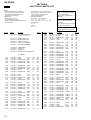
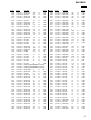
Ref. No. Part No. Description Remark Ref. No. Part No. Description Remark
R
R
5-1. HEAT SINK (MAIN) SECTION
1 X-2025-547-1 PLATE ASSY, ORNAMENTAL
2 2-589-409-01 SHEET, DOUBLE-FACE ADHESIVE
0F901 1-533-743-11 FUSE (BLADE TYPE) (AUTO FUSE) (40A)
0F902 1-533-743-11 FUSE (BLADE TYPE) (AUTO FUSE) (40A)
#1 7-685-545-14 SCREW +BTP 3X6 TYPE2 N-S
#2 7-685-546-19 SCREW +BTP 3X8 TYPE2 N-S
#3 7-685-649-79 SCREW +BVTP 3X14 TYPE2 N-S
The components identified by
mark 0 or dotted line with mark
0 are critical for safety.
Replace only with part number
specified.
Les composants identifiés par une
marque 0 sont critiques pour
la sécurité.
Ne les remplacer que par une piéce
portant le numéro spécifié.
1
2
#1
#1
#2
#2
#2
#2
#2
#3
#3
#2
F901
F902
not supplied
not supplied
not supplied
not supplie
d
not supplied
(LED board)

17
XM-SD22X
Ref. No. Part No. Description Remark Ref. No. Part No. Description Remark
5-2. MAIN BOARD SECTION
51 3-262-163-01 PANEL (FRONT)
52 A-1083-419-A MAIN BOARD, COMPLETE
53 3-238-413-01 SHEET (TR), INSULATING
54 3-225-183-12 SCREW (+PSW.TT.3XL)
55 3-249-786-01 HEAT SINK (SUB.POWER)
56 3-225-183-32 SCREW (+PSW.TT.3XL)
57 3-225-184-12 SCREW (+PS.TT.3XL)
58 3-253-537-01 SCREW (M5X11)
59 3-912-431-01 SCREW (+-P)
60 3-912-432-01 SCREW (+-B)
Q108 X-3383-027-1 FET PAIR ASSY (N) (IRF540) (set of 3)
Q109 X-3383-028-1 FET PAIR ASSY (P) (IRF9540) (set of 3)
Q110 X-3383-027-1 FET PAIR ASSY (N) (IRF540) (set of 3)
Q111 X-3383-028-1 FET PAIR ASSY (P) (IRF9540) (set of 3)
Q112 X-3383-027-1 FET PAIR ASSY (N) (IRF540) (set of 3)
Q113 X-3383-028-1 FET PAIR ASSY (P) (IRF9540) (set of 3)
Q208 X-3383-027-1 FET PAIR ASSY (N) (IRF540) (set of 3)
Q209 X-3383-028-1 FET PAIR ASSY (P) (IRF9540) (set of 3)
Q210 X-3383-027-1 FET PAIR ASSY (N) (IRF540) (set of 3)
Q211 X-3383-028-1 FET PAIR ASSY (P) (IRF9540) (set of 3)
Q212 X-3383-027-1 FET PAIR ASSY (N) (IRF540) (set of 3)
Q213 X-3383-028-1 FET PAIR ASSY (P) (IRF9540) (set of 3)
#4 7-685-646-79 SCREW +P 3X8 TYPE2 NON-SLIT
51
52
56
57
58
59
60
60
57
57
55
53
53
54
54
A
A
#4
#4
not supplied
Q108, 111, 112
Q208, 211, 212
Q209, 210, 213
Q108, 111, 112
not supplied
not supplied
not supplied

18
XM-SD22X
SECTION 6
ELECTRICAL PARTS LIST
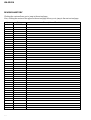
Ref. No. Part No. Description Remark Ref. No. Part No. Description Remark
NOTE:
• Due to standardization, replacements in
the parts list may be different from the
parts specified in the diagrams or the
components used on the set.
• RESISTORS
All resistors are in ohms.
METAL:Metal-film resistor.
METAL OXIDE: Metal oxide-film resistor.
F:nonflammable
• Items marked “*” are not stocked since
they are seldom required for routine service.
Some delay should be anticipated
when ordering these items.
• SEMICONDUCTORS
In each case, u : µ, for example:
uA.. : µA.. uPA.. : µPA..
uPB.. : µPB.. uPC.. : µPC.. uPD.. : µPD..
• CAPACITORS
uF : µF
• COILS
uH : µH
A-1083-419-A MAIN BOARD, COMPLETE
*********************
3-225-183-12 SCREW (+PSW.TT.3XL)
3-225-183-32 SCREW (+PSW.TT.3XL)
3-225-184-12 SCREW (+PS.TT.3XL)
3-238-413-01 SHEET (TR), INSULATING
3-249-786-01 HEAT SINK (SUB.POWER)
3-253-537-01 SCREW (M5X11)
3-912-431-01 SCREW (+-P)
3-912-432-01 SCREW (+-B)
7-685-646-79 SCREW +P 3X8 TYPE2 NON-SLIT
< CAPACITOR >
C101 1-126-794-11 ELECT 4.7uF 20% 50V
C102 1-126-794-11 ELECT 4.7uF 20% 50V
C103 1-162-919-11 CERAMIC CHIP 22PF 5% 50V
C104 1-162-919-11 CERAMIC CHIP 22PF 5% 50V
C105 1-163-251-11 CERAMIC CHIP 100PF 5% 50V
C106 1-163-251-11 CERAMIC CHIP 100PF 5% 50V
C107 1-107-826-11 CERAMIC CHIP 0.1uF 10% 16V
C108 1-107-826-11 CERAMIC CHIP 0.1uF 10% 16V
C109 1-126-796-11 ELECT 22uF 20% 50V
C110 1-162-927-11 CERAMIC CHIP 100PF 5% 50V
C111 1-126-794-11 ELECT 4.7uF 20% 50V
C112 1-126-794-11 ELECT 4.7uF 20% 50V
C116 1-162-927-11 CERAMIC CHIP 100PF 5% 50V
C117 1-126-794-11 ELECT 4.7uF 20% 50V
C118 1-127-715-11 CERAMIC CHIP 0.22uF 10% 16V
C123 1-126-786-11 ELECT 47uF 20% 16V
C124 1-107-826-11 CERAMIC CHIP 0.1uF 10% 16V
C125 1-107-826-11 CERAMIC CHIP 0.1uF 10% 16V
C126 1-162-925-11 CERAMIC CHIP 68PF 5% 50V
C127 1-107-826-11 CERAMIC CHIP 0.1uF 10% 16V
C128 1-137-374-11 MYLAR 0.047uF 5% 50V
C130 1-162-919-11 CERAMIC CHIP 22PF 5% 50V
C131 1-128-499-11 ELECT 220uF 20% 16V
C132 1-162-925-11 CERAMIC CHIP 68PF 5% 50V
C201 1-126-794-11 ELECT 4.7uF 20% 50V
C202 1-126-794-11 ELECT 4.7uF 20% 50V
C203 1-162-919-11 CERAMIC CHIP 22PF 5% 50V
C204 1-162-919-11 CERAMIC CHIP 22PF 5% 50V
C205 1-163-251-11 CERAMIC CHIP 100PF 5% 50V
C206 1-163-251-11 CERAMIC CHIP 100PF 5% 50V
C207 1-107-826-11 CERAMIC CHIP 0.1uF 10% 16V
C208 1-107-826-11 CERAMIC CHIP 0.1uF 10% 16V
C209 1-126-796-11 ELECT 22uF 20% 50V
C210 1-162-927-11 CERAMIC CHIP 100PF 5% 50V
C211 1-126-794-11 ELECT 4.7uF 20% 50V
C212 1-126-794-11 ELECT 4.7uF 20% 50V
C216 1-162-927-11 CERAMIC CHIP 100PF 5% 50V
C217 1-126-794-11 ELECT 4.7uF 20% 50V
C218 1-127-715-11 CERAMIC CHIP 0.22uF 10% 16V
C221 1-115-339-11 CERAMIC CHIP 0.1uF 10% 50V
C222 1-162-927-11 CERAMIC CHIP 100PF 5% 50V
C223 1-126-786-11 ELECT 47uF 20% 16V
C224 1-107-826-11 CERAMIC CHIP 0.1uF 10% 16V
C225 1-107-826-11 CERAMIC CHIP 0.1uF 10% 16V
C226 1-162-925-11 CERAMIC CHIP 68PF 5% 50V
C227 1-107-826-11 CERAMIC CHIP 0.1uF 10% 16V
C228 1-137-374-11 MYLAR 0.047uF 5% 50V
C230 1-162-919-11 CERAMIC CHIP 22PF 5% 50V
C231 1-115-339-11 CERAMIC CHIP 0.1uF 10% 50V
C232 1-162-925-11 CERAMIC CHIP 68PF 5% 50V
C301 1-162-927-11 CERAMIC CHIP 100PF 5% 50V
C302 1-162-927-11 CERAMIC CHIP 100PF 5% 50V
C303 1-127-715-11 CERAMIC CHIP 0.22uF 10% 16V
C304 1-107-826-11 CERAMIC CHIP 0.1uF 10% 16V
C305 1-162-927-11 CERAMIC CHIP 100PF 5% 50V
C701 1-126-796-11 ELECT 22uF 20% 50V
C801 1-127-715-11 CERAMIC CHIP 0.22uF 10% 16V
C802 1-126-786-11 ELECT 47uF 20% 16V
C803 1-162-964-11 CERAMIC CHIP 0.001uF 10% 50V
C804 1-162-962-11 CERAMIC CHIP 470PF 10% 50V
C805 1-126-794-11 ELECT 4.7uF 20% 50V
C806 1-162-964-11 CERAMIC CHIP 0.001uF 10% 50V
C860 1-107-826-11 CERAMIC CHIP 0.1uF 10% 16V
C901 1-115-339-11 CERAMIC CHIP 0.1uF 10% 50V
C902 1-115-339-11 CERAMIC CHIP 0.1uF 10% 50V
C903 1-164-161-11 CERAMIC CHIP 0.0022uF 10% 50V
C904 1-164-161-11 CERAMIC CHIP 0.0022uF 10% 50V
C905 1-164-161-11 CERAMIC CHIP 0.0022uF 10% 50V
C906 1-164-161-11 CERAMIC CHIP 0.0022uF 10% 50V
C907 1-126-786-11 ELECT 47uF 20% 16V
C908 1-162-970-11 CERAMIC CHIP 0.01uF 10% 25V
C909 1-130-471-00 MYLAR 0.001uF 5% 50V
C911 1-126-960-11 ELECT 1uF 20% 50V
C912 1-128-126-11 ELECT 100uF 20% 25V
C913 1-162-964-11 CERAMIC CHIP 0.001uF 10% 50V
The components identified by
mark 0 or dotted line with mark
0 are critical for safety.
Replace only with part number
specified.
Les composants identifiés par une
marque 0 sont critiques pour
la sécurité.
Ne les remplacer que par une piéce
portant le numéro spécifié.
When indicating parts by reference
number, please include the board.
MAIN

19
XM-SD22X
Ref. No. Part No. Description Remark Ref. No. Part No. Description Remark
C914 1-162-964-11 CERAMIC CHIP 0.001uF 10% 50V
C915 1-137-194-81 FILM 0.47uF 5% 50V
C916 1-137-372-11 MYLAR 0.022uF 5% 50V
C917 1-128-951-21 ELECT 2200uF 20% 16V
C918 1-128-951-21 ELECT 2200uF 20% 16V
C919 1-128-951-21 ELECT 2200uF 20% 16V
C920 1-128-951-21 ELECT 2200uF 20% 16V
C921 1-100-199-31 ELECT 2200uF 20% 50V
C922 1-100-199-31 ELECT 2200uF 20% 50V
C923 1-100-199-31 ELECT 2200uF 20% 50V
C924 1-100-199-31 ELECT 2200uF 20% 50V
C925 1-100-199-31 ELECT 2200uF 20% 50V
C926 1-100-199-31 ELECT 2200uF 20% 50V
C927 1-115-339-11 CERAMIC CHIP 0.1uF 10% 50V
C928 1-115-339-11 CERAMIC CHIP 0.1uF 10% 50V
C932 1-104-666-11 ELECT 220uF 20% 25V
C933 1-104-666-11 ELECT 220uF 20% 25V
C934 1-130-495-00 MYLAR 0.1uF 5% 50V
C935 1-130-495-00 MYLAR 0.1uF 5% 50V
C936 1-104-666-11 ELECT 220uF 20% 25V
C937 1-104-666-11 ELECT 220uF 20% 25V
C938 1-128-576-11 ELECT 100uF 20% 63V
C939 1-128-576-11 ELECT 100uF 20% 63V
C940 1-115-339-11 CERAMIC CHIP 0.1uF 10% 50V
C941 1-115-339-11 CERAMIC CHIP 0.1uF 10% 50V
C942 1-162-968-11 CERAMIC CHIP 0.0047uF 10% 50V
C943 1-162-968-11 CERAMIC CHIP 0.0047uF 10% 50V
< TERMINAL BOARD >
CN801 1-694-983-11 TERMINAL BOARD (3P+FUSE)
(REM,+12V,GND,40A,40A)
CN804 1-694-984-11 TERMINAL BOARD (2P) (SPEAKER OUT (L))
CN805 1-694-984-11 TERMINAL BOARD (2P) (SPEAKER OUT (R))
< CONNECTOR >
* CN803 1-691-785-11 PIN, CONNECTOR (PC BOARD) 4P
(HIGH LEVEL INPUT)
CN810 1-506-468-11 PIN, CONNECTOR 3P
< JACK >
CNJ801 1-779-078-41 JACK, PIN 4P (INPUT,OUTPUT (THROUGH))
< DIODE >
D104 8-719-083-60 DIODE UDZSTE-174.7B
D106 8-719-082-03 DIODE MM3Z15VT1
D107 8-719-082-03 DIODE MM3Z15VT1
D108 8-719-080-34 DIODE SDS511
D109 8-719-080-34 DIODE SDS511
D204 8-719-083-60 DIODE UDZSTE-174.7B
D206 8-719-082-03 DIODE MM3Z15VT1
D207 8-719-082-03 DIODE MM3Z15VT1
D208 8-719-080-34 DIODE SDS511
D209 8-719-080-34 DIODE SDS511
D701 8-719-978-33 DIODE DTZ-TT11-6.8B
D702 8-719-080-34 DIODE SDS511
D703 8-719-080-34 DIODE SDS511
D801 8-719-080-34 DIODE SDS511
D802 8-719-080-34 DIODE SDS511
D803 8-719-080-34 DIODE SDS511
D820 8-719-080-34 DIODE SDS511
D822 8-719-080-34 DIODE SDS511
D827 8-719-080-34 DIODE SDS511
D832 8-719-080-34 DIODE SDS511
D901 8-719-978-33 DIODE DTZ-TT11-6.8B
D902 8-719-065-46 DIODE 02DZ16-Z(TPH3)
D905 8-719-079-00 DIODE FCH10A15
D906 8-719-079-01 DIODE FRH10A15
D909 8-719-054-55 DIODE 1SS306-TE85L
D910 8-719-054-55 DIODE 1SS306-TE85L
D911 8-719-079-92 DIODE 1SR159-200TE25
D912 8-719-079-92 DIODE 1SR159-200TE25
D913 8-719-065-46 DIODE 02DZ16-Z(TPH3)
D914 8-719-065-46 DIODE 02DZ16-Z(TPH3)
D915 8-719-065-42 DIODE 02DZ15-Y(TPH3)
D917 8-719-079-92 DIODE 1SR159-200TE25
D918 8-719-079-92 DIODE 1SR159-200TE25
D919 8-719-080-34 DIODE SDS511
D920 8-719-080-34 DIODE SDS511
< FUSE >
0F901 1-533-743-11 FUSE (BLADE TYPE) (AUTO FUSE) (40A)
0F902 1-533-743-11 FUSE (BLADE TYPE) (AUTO FUSE) (40A)
< IC >
IC101 8-759-710-97 IC NJM4565M-D
IC102 8-759-710-97 IC NJM4565M-D
IC202 8-759-710-97 IC NJM4565M-D
IC301 8-759-909-71 IC BA4558F
IC302 8-759-909-71 IC BA4558F
IC901 6-703-643-01 IC TL594INSR
< PHOTO TRANSISTOR >
IC902 6-600-354-01 PHOTO TRANSISTOR PC-17K1
IC903 6-600-354-01 PHOTO TRANSISTOR PC-17K1
< JUMPER RESISTOR >
JR100 1-216-296-11 SHORT CHIP 0
JR103 1-216-296-11 SHORT CHIP 0
JR106 1-216-296-11 SHORT CHIP 0
JR107 1-216-296-11 SHORT CHIP 0
JR204 1-216-295-11 SHORT CHIP 0
JR205 1-216-295-11 SHORT CHIP 0
JR206 1-216-295-11 SHORT CHIP 0
JR207 1-216-295-11 SHORT CHIP 0
JR208 1-216-295-11 SHORT CHIP 0
JR215 1-216-295-11 SHORT CHIP 0
JR216 1-216-295-11 SHORT CHIP 0
JR217 1-216-295-11 SHORT CHIP 0
< COIL >
L901 1-456-139-12 INDUCTOR 35uH
L902 1-410-396-71 FERRITE 0.45uH
L903 1-456-139-12 INDUCTOR 35uH
L904 1-410-396-71 FERRITE 0.45uH
L905 1-410-396-71 FERRITE 0.45uH
The components identified by
mark 0 or dotted line with mark
0 are critical for safety.
Replace only with part number
specified.
Les composants identifiés par une
marque 0 sont critiques pour
la sécurité.
Ne les remplacer que par une piéce
portant le numéro spécifié.
MAIN

20
XM-SD22X
Ref. No. Part No. Description Remark Ref. No. Part No. Description Remark
L906 1-410-396-71 FERRITE 0.45uH
L907 1-410-396-71 FERRITE 0.45uH
L908 1-410-396-71 FERRITE 0.45uH
< THERMISTOR (POSITIVE) >
PTH801 1-805-163-21 THERMISTOR, POSITIVE
< TRANSISTOR >
Q101 8-729-034-51 TRANSISTOR KTC3875
Q102 6-550-686-01 TRANSISTOR KTC2875-B-RTK
Q103 6-550-031-01 TRANSISTOR HN4C06J-GRBL(TE85R)
Q104 6-550-032-01 TRANSISTOR HN4A06J-GRBL(TE85R)
Q105 6-550-691-01 TRANSISTOR KTA1045L-Y
Q106 6-550-692-01 TRANSISTOR KTC2025L-Y
Q107 8-729-041-66 TRANSISTOR 2SC4015TV2
Q108 X-3383-027-1 FET PAIR ASSY (N) (IRF540) (set of 3)
Q109 X-3383-028-1 FET PAIR ASSY (P) (IRF9540) (set of 3)
Q110 X-3383-027-1 FET PAIR ASSY (N) (IRF540) (set of 3)
Q111 X-3383-028-1 FET PAIR ASSY (P) (IRF9540) (set of 3)
Q112 X-3383-027-1 FET PAIR ASSY (N) (IRF540) (set of 3)
Q113 X-3383-028-1 FET PAIR ASSY (P) (IRF9540) (set of 3)
Q114 8-729-034-51 TRANSISTOR KTC3875
Q201 8-729-034-51 TRANSISTOR KTC3875
Q202 6-550-686-01 TRANSISTOR KTC2875-B-RTK
Q203 6-550-031-01 TRANSISTOR HN4C06J-GRBL(TE85R)
Q204 6-550-032-01 TRANSISTOR HN4A06J-GRBL(TE85R)
Q205 6-550-691-01 TRANSISTOR KTA1045L-Y
Q206 6-550-692-01 TRANSISTOR KTC2025L-Y
Q207 8-729-041-66 TRANSISTOR 2SC4015TV2
Q208 X-3383-027-1 FET PAIR ASSY (N) (IRF540) (set of 3)
Q209 X-3383-028-1 FET PAIR ASSY (P) (IRF9540) (set of 3)
Q210 X-3383-027-1 FET PAIR ASSY (N) (IRF540) (set of 3)
Q211 X-3383-028-1 FET PAIR ASSY (P) (IRF9540) (set of 3)
Q212 X-3383-027-1 FET PAIR ASSY (N) (IRF540) (set of 3)
Q213 X-3383-028-1 FET PAIR ASSY (P) (IRF9540) (set of 3)
Q214 8-729-034-51 TRANSISTOR KTC3875
Q701 6-550-690-01 TRANSISTOR KTA1661
Q702 8-729-034-51 TRANSISTOR KTC3875
Q801 8-729-034-50 TRANSISTOR KTA1504
Q802 8-729-034-51 TRANSISTOR KTC3875
Q803 8-729-034-50 TRANSISTOR KTA1504
Q804 8-729-034-51 TRANSISTOR KTC3875
Q805 8-729-034-50 TRANSISTOR KTA1504
Q806 8-729-034-51 TRANSISTOR KTC3875
Q809 6-550-693-01 TRANSISTOR KTC4373
Q901 8-729-052-82 TRANSISTOR KTA1281Y-AT
Q902 8-729-034-50 TRANSISTOR KTA1504
Q903 8-729-034-51 TRANSISTOR KTC3875
Q904 6-550-341-01 FET FKV550N
Q905 6-550-341-01 FET FKV550N
Q906 6-550-341-01 FET FKV550N
Q907 6-550-341-01 FET FKV550N
Q908 6-550-341-01 FET FKV550N
Q909 6-550-341-01 FET FKV550N
Q910 6-550-693-01 TRANSISTOR KTC4373
Q911 6-550-693-01 TRANSISTOR KTC4373
Q912 8-729-034-51 TRANSISTOR KTC3875
Q913 8-729-034-51 TRANSISTOR KTC3875
Q914 6-550-693-01 TRANSISTOR KTC4373
Q915 6-550-690-01 TRANSISTOR KTA1661
Q920 6-550-693-01 TRANSISTOR KTC4373
< RESISTOR >
R101 1-216-837-11 METAL CHIP 22K 5% 1/10W
R102 1-216-837-11 METAL CHIP 22K 5% 1/10W
R103 1-216-837-11 METAL CHIP 22K 5% 1/10W
R104 1-216-837-11 METAL CHIP 22K 5% 1/10W
R105 1-216-206-00 RES-CHIP 2.2K 5% 1/8W
R106 1-216-845-11 METAL CHIP 100K 5% 1/10W
R107 1-216-845-11 METAL CHIP 100K 5% 1/10W
R108 1-216-833-11 METAL CHIP 10K 5% 1/10W
R109 1-216-033-00 RES-CHIP 220 5% 1/10W
R110 1-216-845-11 METAL CHIP 100K 5% 1/10W
R111 1-216-845-11 METAL CHIP 100K 5% 1/10W
R120 1-216-077-11 RES-CHIP 15K 5% 1/10W
R121 1-216-843-11 METAL CHIP 68K 5% 1/10W
R122 1-216-295-11 SHORT CHIP 0
R123 1-216-827-11 METAL CHIP 3.3K 5% 1/10W
R124 1-216-045-00 RES-CHIP 680 5% 1/10W
R125 1-216-837-11 METAL CHIP 22K 5% 1/10W
R126 1-216-829-11 METAL CHIP 4.7K 5% 1/10W
R129 1-216-841-11 METAL CHIP 47K 5% 1/10W
R130 1-216-829-11 METAL CHIP 4.7K 5% 1/10W
R131 1-216-829-11 METAL CHIP 4.7K 5% 1/10W
R132 1-216-829-11 METAL CHIP 4.7K 5% 1/10W
R133 1-216-077-11 RES-CHIP 15K 5% 1/10W
R134 1-216-077-11 RES-CHIP 15K 5% 1/10W
R135 1-216-033-00 RES-CHIP 220 5% 1/10W
R136 1-216-033-00 RES-CHIP 220 5% 1/10W
R138 1-216-821-11 METAL CHIP 1K 5% 1/10W
R139 1-216-845-11 METAL CHIP 100K 5% 1/10W
R140 1-216-845-11 METAL CHIP 100K 5% 1/10W
R141 1-249-421-11 CARBON 2.2K 5% 1/4W
R142 1-249-428-11 CARBON 8.2K 5% 1/4W
R143 1-216-017-11 RES-CHIP 47 5% 1/10W
R144 1-216-017-11 RES-CHIP 47 5% 1/10W
R145 1-216-017-11 RES-CHIP 47 5% 1/10W
R146 1-216-017-11 RES-CHIP 47 5% 1/10W
R147 1-216-017-11 RES-CHIP 47 5% 1/10W
R148 1-216-017-11 RES-CHIP 47 5% 1/10W
R149 1-234-499-11 ENCAPSULATED COMPONENT 0.22X2 5W
R150 1-234-499-11 ENCAPSULATED COMPONENT 0.22X2 5W
R151 1-234-499-11 ENCAPSULATED COMPONENT 0.22X2 5W
R152 1-215-880-31 METAL OXIDE 10 5% 2W F
R153 1-216-853-11 METAL CHIP 470K 5% 1/10W
R154 1-216-065-11 RES-CHIP 4.7K 5% 1/10W
R155 1-216-829-11 METAL CHIP 4.7K 5% 1/10W
R156 1-216-829-11 METAL CHIP 4.7K 5% 1/10W
R160 1-216-827-11 METAL CHIP 3.3K 5% 1/10W
R161 1-216-821-11 METAL CHIP 1K 5% 1/10W
R201 1-216-837-11 METAL CHIP 22K 5% 1/10W
R202 1-216-837-11 METAL CHIP 22K 5% 1/10W
R203 1-216-837-11 METAL CHIP 22K 5% 1/10W
R204 1-216-837-11 METAL CHIP 22K 5% 1/10W
R205 1-216-206-00 RES-CHIP 2.2K 5% 1/8W
R206 1-216-845-11 METAL CHIP 100K 5% 1/10W
MAIN
La page est en cours de chargement...
La page est en cours de chargement...
La page est en cours de chargement...
La page est en cours de chargement...
-
 1
1
-
 2
2
-
 3
3
-
 4
4
-
 5
5
-
 6
6
-
 7
7
-
 8
8
-
 9
9
-
 10
10
-
 11
11
-
 12
12
-
 13
13
-
 14
14
-
 15
15
-
 16
16
-
 17
17
-
 18
18
-
 19
19
-
 20
20
-
 21
21
-
 22
22
-
 23
23
-
 24
24


Sony XM SD22X Manuel utilisateur
- Taper
- Manuel utilisateur
- Ce manuel convient également à
Documents connexes
Autres documents
-
Compaq NSZ2107STTUW Manuel utilisateur
-
Hitachi HMA-6500 Manuel utilisateur
-
iGuzzini R956 Guide d'installation
-
-
-
-
-
-
-
Logitech 960-001176 Manuel utilisateur