Hitachi C1422R Manuel utilisateur
- Catégorie
- Téléviseurs LCD
- Taper
- Manuel utilisateur

TECHNICAL SPECIFICATIONS
SPÉCIFICATIONS TECHNIQUES
SPECIFICATIONS TECHNIQUES
TV Standard.......................................625 lines,
STANDARD I (UK)
B/G/H/DK, L/L', (Export)
Channel coverage..............UHF Channels (UK)
UHF/VHF Hyper band (Export)
Aerial input impedance.......................... 75ohm
Unbalanced
Power Consumption ..................... Picture Tube
14” Models < 40W 35.5cm types
20” Models < 48W 48cm types
21” Models < 52W 51cm types
Standard TV.....................................625 lignes,
STANDARD: R-U
B/G/H/DK, L/L': (Export)
Couverture de canaux......... Canaux UHF (R-U)
UHF/VHF Band hyper (Export)
Impédance d'entrée d'antenne............ 75 ohms
Non équilibrée
Consommation électrique.......... Tubes-images
14” Models < 40W 35.5cm types
20” Models < 48W 48cm types
21” Models < 52W 51cm types
Fernsehnorm....................................625 Zeilen,
Fernsehnorm I (nur GB)
Fernsehnorm B/G/H/DK, L/L’ (Export)
Kanäle.................................. UHF-Bereich (GB)
UHF/VHF/Hyperband Bereich
Antenneneingangsimpedanz .............. 75 ohms
Unsymmetrisch
Leistungsaufnahme ............................Bildröhre
14” Models < 40W 35.5cm types
20” Models < 48W 48cm types
21” Models < 52W 51cm types
Consumption in standby mode.................<4W
Mains Voltage ........................220V/210V, 50Hz
Fuse..........................................2 Amp time-lag
Consommation en mode veille .................<4W
Tention secteur ......................220V/240V, 50Hz
Fusible......................................2 Amp time-lag
Leistungsaufnahme im standby mode......<4W
Netzspannung .........................220/240V, 50Hz
Sicherung..................................2 Amp time-lag
December 1998
No. 0102
Model Chassis
C1422R F1R
C1422T F1Y
C2122T F4Y
CP1422R F1GR
CP2122R F4GR
CP1422T F1GY
CP2022T F2GY
CP2122T F4GY
CP1422T-481 F1HY
CP2122T-481 F4HY
CP1422T-491 F1HY
CP2022T-491 F2HY
CP2122T-491 F4HY
CS1422R F1KR
CS2022R F2KR
CS2122R F4KR
CL1422R F1FR
CL2122R F4FR
SERVICE MANUAL
MANUEL D’ENTRETIEN
WARTUNGSHANDBUCH
CAUTION:
Before servicing this chassis, it is important that the service technician read
the “Safety Precautions” and “Product Safety Notices” in this service manual.
ATTENTION:
A
vant d’effectuer l’entretien du châassis, le technicien doit lire les
«Précautions de sécurité» et les «Notices de sécurité du produit» présentés
dans le présent manuel.
VORSICHT:
Vor Öffnen des Gehäuses hat der Service-Ingenieur die „Sicherheitshinweise“
und „Hinweise zur Produktsicherheit“ in diesem Wartungshandbuch zu lesen.
Data contained within this Service
manual is subject to alteration for
improvement.
Les données fournies dans le
présent manuel d’entretien
peuvent faire l’objet de
modifications en vue de
perfectionner le produit.
Die in diesem Wartungshandbuch
enthaltenen Spezifikationen
können sich zwecks
V
erbesserun
g
en ändern.

2

3
ENGLISH
SAFETY PRECAUTIONS
WARNING: The following precautions must be observed.
ALL PRODUCTS
Before any service is performed on the chassis an
isolation transformer should be inserted between the
power line and the product.
1. When replacing the chassis in the cabinet, ensure
all the protective devices are put back in place.
2. When service is required, observe the original
lead dressing. Extra precaution should be taken to
ensure correct lead dressing in any high voltage
circuitry area.
3. Many electrical and mechanical parts in
HITACHI products have special safety related
characteristics. These characteristics are often not
evident from visual inspection, nor can the
protection afforded by them necessarily be
obtained by using replacement components rated
for higher voltage, wattage, etc. Replacement
parts which have these special safety
characteristics are identified by marking with a
! on the schematics and the replacement parts
list.
The use of a substitute replacement component
that does not have the same safety characteristics
as the HITACHI recommended replacement one,
shown in the parts list, may create electrical
shock, fire, X-radiation, or other hazards.
4. Always replace original spacers and maintain lead
lengths. Furthermore, where a short circuit has
occurred, replace those components that indicate
evidence of overheating.
5. Insulation resistance should not be less than 2M
ohms at 500V DC between the main poles and
any accessible metal parts.
6. No flashover or breakdown should occur during
the dielectric strength test, applying 3kV AC or
4.25kV DC for two seconds between the main
poles and accessible metal parts.
7. Before returning a serviced product to the
customer, the service technician must thoroughly
test the unit to be certain that it is completely safe
to operate without danger of electrical shock. The
service technician must make sure that no
protective device built into the instrument by the
manufacturer has become defective, or
inadvertently damaged during servicing.
CE MARK
1. HITACHI products may contain the CE mark on
the rating plate indicating that the product
contains parts that have been specifically
approved to provide electromagnetic
compatibility to designated levels.
2. When replacing any part in this product, please
use only the correct part itemised in the parts list
to ensure this standard is maintained, and take
care to replace lead dressing to its original state,
as this can have a bearing on the electromagnetic
radiation/immunity.
PICTURE TUBE
1. The line output stage can develop voltages in
excess of 25kV; if the E.H.T. cap is required to be
removed, discharge the anode to chassis via a
high value resistor, prior to its removal from the
picture tube.
2. High voltage should always be kept at the rated
value of the chassis and no higher. Operating at
higher voltages may cause a failure of the picture
tube or high voltage supply, and also, under
certain circumstances could produce X-radiation
levels moderately in excess of design levels. The
high voltage must not, under any circumstances,
exceed 29kV on the chassis (except for projection
Televisions).
3. The primary source of X-radiation in the product
is the picture tube. The picture tube utilised for
the above mentioned function in this chassis is
specially constructed to limit X-radiation. For
continued X-radiation protection, replace tube
with the same type as the original HITACHI
approved type
4. Keep the picture tube away from the body while
handling. Do not install, remove, or handle the
picture tube in any manner unless shatterproof
goggles are worn. People not so equipped should
be kept away while picture tubes are handled
LASERS
If the product contains a laser avoid direct exposure to
the beam when the cover is open or when interlocks are
defeated or have failed.

4
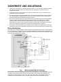
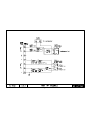
SAFETY AND ISOLATION
1. Under no circumstances should any form of repair or maintenance be attempted by any person other than a
competent technician or engineer. The following precautions should be observed:
2. For purposes of servicing, the chassis should be supplied from an isolation transformer of at least 150W rating.
3. If disturbed, the original lead dressing should be restored. This is particularly important due to the 'hot coil'
nature of the chassis. Lead dressing will also have a bearing on the EMC performance of the chassis.
4. Components marked ! on the circuit diagram are safety approved types and have special safety related
characteristics. Only the manufacturers replacement components should be used. Replacement with alternative
or 'up-rated' parts e.g. higher power resistors definitely does not guarantee the same level of protection and
may create a fire, electric shock or X-radiation hazard.
5. Components not bearing the ! mark should still be replaced with the originally fitted type and should be
mounted in the same way.
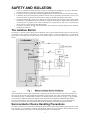
The Isolation Barrier
The chassis is a 'hot-coil' chassis whereby the line deflection coils are NOT isolated from the mains since the PSU does
not provide B+ rail isolation. Consequently, the mains isolation barrier is more convoluted than in a conventional
chassis and a much larger portion of the chassis is non-isolated. Figure 1 shows the isolation barrier position in the
chassis.
It can be seen that both the DST (T401) and the scan coils now straddle the isolation barrier and are, as such, safety
critical components. Also, the opto-coupler (I402) is required to pass line drive from I501 on the 'cold' side to the line
drive stage on the 'hot' side. The isolation barrier therefore consists of T802, T401, I402, C804, R804, R805, the scan
coils and 6mm air gaps. To maintain barrier integrity care should be taken not to reduce any air gaps, e.g. by protruding
wires, following component replacement. Deflection yoke lead dressing is important to maintain double insulation
across the isolation barrier. The position of the deflection lead sleeving is maintained by a tie wrap. Should this be
removed for any reason, the sleeving should be slid towards the deflection yoke and tie wrapped into position.
Semiconductor Device Handling Precautions
The chassis contains devices which may be damaged by static electrical charge during handling, particularly I501, I602,
I701 and Q801. To avoid damage, soldering irons should be earthed and service engineers should ideally wear wrist
straps earthed through a 1M resistor or at least discharge themselves to an earthed point.

5
S
ERVICING
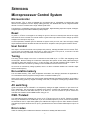
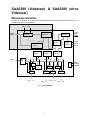
Microprocessor Control System
Microcontroller
Micro-controller, I701, is either a SAA5288 (on non-teletext sets) or a SAA5290 (on teletext sets). Both
devices have integrated on-screen display (OSD) generator; the SAA5290 also has an integrated teletext
decoder. The micro-controller has a single 12MHz crystal X701.
The television is controlled by serial (I²C) bus communication, digital switching inputs and outputs, analogue-
to-digital inputs and pulse-width-modulation (PWM) outputs.
Reset
At power on, C709 is not charged so the voltage on pin 43 of the micro-controller rises with the 5V supply
and resets the micro-controller. An internal resistor to ground at this pin causes C709 to charge up and the
voltage on the reset pin to drop to 0V.
In normal operation, transistor Q702 is switched on and the reset pin is low, but if the 10V supply voltage
drops below about 8V the transistor will switch off and R721 will pull the reset pin high and reset the device.
User Control
User input is via infra-red remote control (Philips' RC5 protocol), internally decoded from the receiver I703,
or from three (non-matrixed) local control keys on active low inputs, I701 pins 18, 19 and 20. The LED
flashes each time a key is detected or remote command received.
Tuning
The tuning control voltage to the tuner is controlled via the PWM at pin 1 of I701 and integrating circuit
around Q001. Minimum voltage is at maximum mark-space ratio (bottom of each band). Band-switching is
controlled by active low outputs on pins 14, 15 and 16 (high, mid, low) and transistors Q002 to Q004. The
controller makes AFC corrections by reading on-tune information from I501 via the I²C bus.
As the tuner is controlled by voltage synthesis, there is no direct correlation between the controller output
and the tuned frequency.
Non-volatile memory
The non-volatile memory, I702, holds configuration information, user settings, parameters as applicable for
I²C controlled ICs and the programme tuning records. It is itself accessed by I²C.
When a new memory IC is fitted, the microcontroller will automatically load default information, which takes a
few seconds during power-up. Regular re-loading of the data, or corruption of settings may indicate I702 is
faulty.
AV switching
Inputs from pins 8 and 16 of SCART 1 are sampled by analogue to digital conversion on pins 9 and 10 of
I701 respectively. The input levels are adjusted such that the controller will automatically switch to AV1
when pin 8 is above 6V and RGB when pin 16 is above 1V. The time constant on pin 16 ensures the
controller will not detect real-time RGB insertion using pin 16.
OSD / Teletext
Line and field timings are obtained from V.sync on pin 37 and H.sync input on pin 36. Teletext (on teletext
sets only) is obtained from the CVBS input on pin 23. The RGB outputs on pins 34, 33 and 32 respectively
are inserted into the TV output when gated by the OSD EN OUT signal on pin 35. OSD / teletext contrast is
controlled by the peak reference level on pin 31, generated from the microcontroller PWM output on pin 2 via
Q305.
Error codes
Under the following fault conditions the television will switch to standby and flash the LED.

6
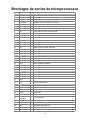
Fault Condition No. of Flashes
Multiple TDA884X I²C errors 1
Over voltage / X-ray protection (OVP) 2
Line start-up sequence failed 3
Black current (BC) loop unstable 4
Vertical scan failure 5
Continuous TDA884X power-on reset 6
Multiple error codes may appear, eg. two quick flashes, pause, four quick flashes etc. for OVP + BC loop
errors.
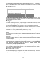
Adjustments
In order to make service adjustments including setting the height, width, various configuration options, etc.,
the TV should have a suitable signal tuned in; ideally, a geometry test card. A teletext signal is
recommended for setting OSD contrast on a teletext chassis.
To enter service mode, place a shorting link across terminals 2 and 3 of P701.
In service mode, two 2-digit hexadecimal numbers are displayed to the left of the screen; the lefthand one is
the service parameter number, the righthand one is the value for that parameter. Some parameters are
identified by a two-letter code instead of a number, see below.
For example:- 0A 1F shows parameter ten (0A hex) at thirty-one (1F hex).
In this mode of operation some of the remote control keys have different functions;
The up and down and local select keys are used to select a parameter.
The remote and local left and right keys are used to change the value of the current parameter.
The TV button is used to store any changes.
The teletext select and digit '0' keys are used for programme up or down.
The Normalize key selects factory picture settings immediately over-writing user settings.
The digit keys '1', '2',----'8' toggle the state of the individual bits '7', '6',----'0' of the value of the current
parameter, for example, pressing digit key '4' would change value 1F hex to 0F hex.
TO STORE THE CHANGES, PRESS THE TV KEY ON THE HAND UNIT BEFORE REMOVING THE
SERVICE MODE LINK. THE MESSAGE 'STORED' WILL BE DISPLAYED TO CONFIRM THE
OPERATION.
Under certain circumstances, for example abnormal operation due to suspected corruption of the service
parameters, it may be necessary to perform a complete reset of the non-volatile memory (I702). To effect
this, press and hold the X (teletext update) key for about 3 seconds or until the set switches to standby.
Following this it will be necessary to perform a 'set-up' of the television.
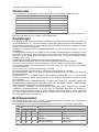
Service Parameters
The following values assume you are watching a tuned in picture, on RF. (On other sources, or with no
signal, some values may differ.)
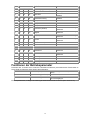
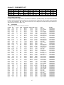
Service parameters 00 to 1A apply to the control registers of I501 as shown in the following table.
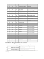
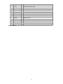
No. Value Function Action
14" 20" 21"
00 02 02 02 System Control Do not adjust
01 D0 D0 D0 System Control Do not adjust
02 1F 1F 1F Hue (SCART NTSC 4.43 playback only) Use picture menu control instead
03 20 1D 27 Horizontal shift Adjust to centre picture horizontally
04-07 00 0 0 00 E-W control Not used on this chassis
08 20 1F 1E Vertical slope (linearity) Adjust for vertical linearity
09 10 0B 1A Height Adjust for correct picture height
0A 44 4A 4A S-correction Adjust for best vertical S-correction

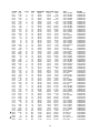
7
No. Value Function Action
14" 20" 21"
0B 2B 1B 1B Vertical shift Adjust to centre picture vertically
0C 29 38 3D White point - Red
0D 29 38 3D White point - Green
See "Adjustments" in Servicing
0E 29 38 3D White point - Blue
0F 1C 1C 1C Peaking (sharpness) Use picture menu control instead
10 5C 5C 5C Brightness Use picture menu control instead
11 9C 9C 9C Saturation Use picture menu control instead
12 1C 1C 1C Contrast Use picture menu control instead
13 13 13 13 AGC take-over point
See "Adjustments" in Servicing
14 0A 0A 0A Volume
15 50 50 50 IF PLL adjustment Set to 50 hex
16 19 19 19 Vertical zoom Not used on this chassis
17 20 20 20 Vertical scroll Not used on this chassis
18 81 81 81 Control 2 Do not adjust
19 08 08 08 Control 3 Do not adjust
1A 00 00 00 Control 4 Do not adjust
Service Parameter Functions
Parameters above 1A are designated by two-letter codes (except text contrast on a teletext set). These
control configuration.
Text Mode Text (OSD) contrast Set as preferred, see notes below
Ex Export (VHF/UHF) setting 00 for UHF-only, 01 if multi-band tuner
AV AV socket configuration 00 single SCART, 01 single SCART plus phono inputs
It is advisable to make a note of the existing values prior to commencing servicing. (see "Adjustments" in
Servicing)

8
Adjustments
H. T. Setting
The HT should be adjusted using R818 to obtain correct width with normal brightness and contrast settings.
A Philips complex test pattern is ideal for the operation.
A1 Control
This should be set using the ‘screen’ control on T401 to achieve 140V black level at the tube base cathodes
with the brightness and contrast settings normalized. In practice the black level of the individual guns will
differ and are set by I501 to achieve equal cut-off points.
White Points
These should be adjusted via service parameters 0C, 0D and CE whilst viewing a picture with little light area
to prevent beam current limiting. The parameters should be adjusted for a black to white swing of 50V ±1V
(14”), 55V ±1V (20”) or 60V ±1V (21”) on each of the three cathodes with the picture normalized.
Text Contrast
White balancing of the red and blue outputs, relative to the green, should be carried out to ensure pure white
text, using RV317 (R) and RV319 (B). As the picture outputs are automatically balanced, text white may be
set using picture white as a reference once the black and white points (See adjustments section) have been
set. The text contrast itself should be adjusted such, that the Text/OSD white parts are approximately 75% of
the intensity of a test pattern peak white area: this corresponds to the 75% grey blocks in part of a ‘Philips
5544’ type test pattern. When the text contrast service parameter is selected the TV switches to teletext mix
mode, page 101. If no text is present P100 will still appear in the top left corner of the screen together with
some text on the bottom row of the display. There is no on-screen parameter: adjust with volume control as
normal and change parameter with programme up/down keys.
AGC
The AGC take-over point should be adjusted via service parameter 13 such, that the tuner output to the
SAW filter is 600mV pk-pk (300mV per side for symmetrical tuner output) using a test pattern with no sound
carrier.
Focus
Adjust the upper control on the rear of the flyback transformer for best focus.
Positioning
Horizontal position should be adjusted via service parameter 03 so as to centre the picture. Vertical position
should be adjusted via service parameter 0B so as to centre the picture. This may be simplified by pressing
‘1’ with service parameter 0B selected to activate service blanking which blanks the lower half of the picture.
The edge of the blanked area may then be aligned with the tube centre marks. Service blanking is disabled
by once again pressing the ‘1’ key.
Linearity
Horizontal linearity is fixed; no adjustment is possible. Vertical linearity is adjusted using service parameters
08 and 0A (linearity and S-correction) whilst displaying a cross hatch pattern. Adjust the linearity for evenly
spaced intervals at the top and bottom of the picture, then adjust the S-correction to achieve equal spacing
accross the whole screen.
Vertical Protection Disable
Vertical protection is used to shut down the chassis in the event of field-scan failure. For diagnostic purposes
this can be disabled by selecting service parameter OA (S-correction) and pressing the number 2 key on the

9
hand unit. After repair, vertical protection should always be re-enabled by pressing the number 2 key again
and storing it with the TV key. (The value of parameter OA toggles between two values when the number 2
key is pressed,
the higher
of which indicates that the vertical protection is
enabled
.).
Auto Black Level Disable
I501 independently sets the black level of each CRT gun to equalize the cut-off points and therefore provide
a true black. For diagnostic purposes this control loop may be disabled by selecting service parameter 02
(hue) and pressing the number 2 key on the hand unit. After repair, the auto black level sampling should
always be re-enabled by pressing the number 2 key again and storing it with the TV key. (The value of
parameter 02 toggles between two values when the number 2 key is pressed,
the lower
of which indicates
black level sampling is
enabled
).
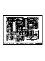
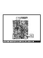
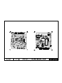
Adjustment Locations (Physical)
See adjustment locations PCB

10
C
IRCUIT
D
ESCRIPTION
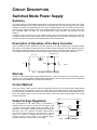
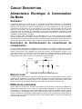
Switched Mode Power Supply
Summary
The power supply is a self-oscillating discontinuous buck converter (step-down chopper) under peak current
control and designed for up to 65W output power at nominally 98V. The main B+ output of this converter
topology is inherently non-isolated and as such, output voltage feedback does not require an opto-coupler.
Some energy is derived in flyback mode via an isolated winding on the buck inductor to provide a low power
10V secondary supply from which are derived switched 8V (video processor) and permanent 5V (µP)
supplies.
In stand-by mode, both the B+ and 10V supplies remain close to their nominal operating levels but with
virtually zero load, the PSU enters a burst-mode whereby typically 180 in 200 cycles are skipped. In this way,
the stand-by power consumption (including degaussing circuit) is less than 4W.
Description of Operation of the Buck Converter
Figure 4 shows the main components of the buck converter. The output voltage may be controlled between
zero and the input voltage by varying the on-time of Q801. During this period, Vin-Vout is applied across the
buck inductor (T802 winding pins 7 & 8) and the current in it ramps up linearly. When Q801 is turned off, -
Vout is applied across the buck inductor and energy is delivered to the load and C809 combination.
Start-Up
At start-up, the overwind output voltage (T802 winding pins 7 & 8) is not present so a start-up bias circuit is
required. This consists of R806, D802 and R809. Approximately 16V is produced at the junction of R806 and
D802 which is fed via R809 to turn on Q801 for the first time.
Control Method
During the on-time of Q801, the buck inductor voltage flows through the current sense resistor R814 forming
an analogue of the buck inductor current. This is fed to the base of Q802 along with a DC bias current from
the error amplifier (via R813) such that once a certain buck inductor current level is reached, Q802 turns on.
When this happens Q801 is turned off and the inductor current free-wheels through D804. This is peak
current-mode control.
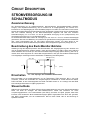
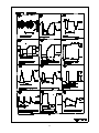
Output Voltage Regulation
The non-isolated B+ rail means that no opto-isolator is
required for direct Vo control. It can be seen from Figure 5 that
Vo minus a small zener voltage drives the emitter of this
transistor (Vo-Vz) whilst a resistive potential divider feeds the
base (kVo, k<1). If, for instance, the output voltage tends to
rise, Ve rises by ∆Vo whereas Vb only rises by ∆kVo. The net
result is an increase in negative bias and an increase in
collector (control) current. R818 in the potential divider
provides an element of control over the B+ voltage.
V
IN
280 - 390
T802 (pins 7 & 8)
Q801
D804
C809
V
OUT
(100V)
R817
Vz
Ve
kVo
Vb
D806
R818
R815
R820
Control Current
Fig 5
The Error Amplifier
Fig 4
The Buck Converter Topology

11
Overvoltage Protection
An unfortunate characteristic of the buck converter is that if the power switch Q801 should become short-
circuit, the full rectified mains voltage appears at the output, over stressing components in both the PSU itself
and the load. In order to limit the output voltage rise under these conditions, a 130V 5W zener diode D805 is
fitted across the B+ output. An over-voltage causes conduction of D805, shorting the B+ output and blowing
the fuse F801.
Isolated Supplies
In order to provide low voltage isolated supplies, a secondary winding is included on the buck inductor,
phased such that energy is delivered in flyback mode, that is when Q801 is off. During this interval, the buck
inductor voltage is clamped to the output voltage and the turns ratio is chosen to provide a secondary of 10V
with rectification and smoothing performed by D807 and C812 and overload protection by R821. A
permanent 5V µP supply is derived from this 10V supply by I801 as well as an 8V switched supply under µP
control by Q804, R822, D808 and Q805.
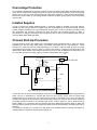
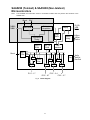
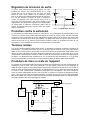
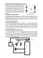
Chassis Start-Up Procedure
The PSU topology used in the chassis has a characteristic which complicates start-up. Until a B+ load is
established (i.e. the line output stage starts), the isolated secondaries are very high impedance - simply
turning on the video processor 8V supply and waiting for line-drive to start-up would fail since the supply
cannot deliver I501's supply current. In order to overcome this problem, a system of 'pseudo line-drive' was
devised which allows the line output stage to be driven by the µP in order to establish a B+ load prior to turn-
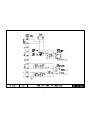
on of the video processor 8V supply. Figure 6 is a block representation of this system.
The two line drive sources are OR-ed together at the input of I402, the two driver transistors being Q402 and
Q406. The µP is responsible for ensuring that both line drive sources cannot drive the output stage
simultaneously and to achieve this, the true line drive from I501 is monitored (µP pin 47). In this way, the
transition from pseudo to true line-drive is timed to the latter starting up. However, the line-drive stage does
not reliably operate at 31kHz so the soft-start cycle of I501 must be gated out. The µP achieves this by
keeping Q405 on for a fixed time after true line-drive has been detected thus keeping Q402 off. When this
time has elapsed, pseudo line-drive is stopped and Q405 turned off simultaneously, completing the start-up
sequence.
On reverting to stand-by pin 7 reverts to the high state which maintains I402 in conduction via Q406. This
maintains Q403 on and the line output transistor (Q404) off.
8V
48
8V
8V Control
12, 37
I501
40
H
OUT
7
Pseudo
Line
Drive
I701
30
True Line
Drive
Gating
47
True Line
Drive
Detection
10V from PSU
Q804, R822, D808, Q805
Q402, R423
Q406, R427
True Line
Q405, R422
I4
0
2
Fig 6
Start-up Circuit Block Diagram

12
Tuner and IF Stages
Tuner
The main chassis is fitted with a voltage synthesis UHF tuner for system I. Control of the tuned frequency is
achieved by a voltage on pin 2 of the tuner. This voltage is derived from integrating a 33 volt PWM switched
waveform. This PWM waveform is derived from pin 1 of the microcontroller I701.
The AFC is sampled by the microcontroller via the I²C bus from I501 and frequency correction is achieved by
microcontroller adjustment of the duty cycle of the PWM which then modifies the tuner frequency.
AGC Adjustment
For most aerial input signal levels the tuner operates at maximum gain. At high signal levels the gain of the
tuner is reduced by an AGC voltage generated in the IF stage. The AGC output from the IF (pin 54 of I501) is
applied to pin 1 of the tuner (H001).
The AGC maintains a maximum IF voltage of 600mV peak to peak. The voltage level can be adjusted using
the following procedure:
Short circuit pins 2 and 3 of P701 to enter service mode. When in service mode use the programme up and
down keys to select service parameter 13. Using a 40MHz or greater oscilloscope, monitor pin 11 of TU001.
Adjust service parameter 13 using the volume up and down keys for 600mV on pin 11 for a single ended
tuner, and 300mV for a differential output tuner. Press the RV key to store the AGC value.
AFC Adjustment
The AFC voltage is not available at any point on the chassis; it is read by the microcontroller via the I²C bus.
Therefore, one of the following methods can be used to correctly align the AFC.
a) For demodulator tank coil fitted (I501 = TDA884X Mask 1)
Tune a known channel. Using a spectrum analyzer monitor pin 11 of H001. Fine tune the tuner for a
carrier frequency of 38.9MHz. Store the fine tuned frequency (i.e. AFC off). Enter service mode by
applying a short circuit to pins 2 and 3 of P701. When in service mode use the programme up and
down keys to select service parameter 15. Adjust service parameter 15 using the volume up and
down keys until the two bits at the top right of the screen meet the following criteria:
Left hand bit permanently set.
Right hand bit toggles (either 1 to 0 or 0 to 1).
When the AFC value has been set press the TV key to store it.
b) For demodulator tank coil not fitted (I501 = TDA886X Mask 2)
Adjust service parameter 15 using the volume up and down keys until its value is 50.
When the AFC value has been set press the TV key to store it.
Vision Decoding
The majority of the vision and sound, deflection and colour decoding is performed by I501. The IF signal
passes from the tuner through the SAW filter (X001) to filter unwanted frequencies to I501. It is demodulated
internally and the output at pin 6 is buffered by Q501. The sound and vision components are now separated.
Z501 removes the sound from the vision components and Z601/602 filters the FM sound to pin 1 for
demodulation. Video is then fed to the SCART socket output, pin 19 of P501 via Q502.

13
Source Selection
Source selection is controlled by the microcontroller via I²C bus commands. The video processor I501 can
select between internal demodulated CVBS video on its pin 13, external CVBS video (AV1) from pin 20 of
P501 on its pin 17 or, if available, from external CVBS video (AV2) from the yellow phono socket of PA501,
which is applied to pin 11. The internally demodulated CVBS video is always available on pin 19 of P501.
External RGB is selected within I501. Fast blanking pulses from pin 16 of P501 are passed via an OR-ing
circuit of Q301-304 and associated components to pin 26 of I501. This pin controls the state of the RGB
outputs to the tube base pins 19, 20 and 21. It has three possible states:
1) Less than 0.4V Internal RGB from colour decoder.
2) Between 0.4V and 4.0V External RGB from pins 7, 11 and 15.
3) Greater than 4V Output blanked for OSD/Text insertion.
When teletext or OSD is displayed, pin 35 of I703 goes from ground to 5.0 Volts. This signal is passed via
Q301 and causes pin 26 of I501 to enter the third state above, independent of the state of the other inputs to
the OR circuit. During mixed TV/Text mode or whilst the OSD is showing on part of the screen this line will
be switching at a high rate. RGB mode can be selected manually by the user and in this case the open-drain
output on pin 8 of the micro-controller will be switched off and will be pulled up to 1.7 volts by R307 and
R306. Q302 then applies a voltage of about 1.0 volts to pin 26 of I501. In the absence of a higher voltage via
Q301 and Q303 from the fast blanking input, pin 16 of P501, this is still sufficient to enter the external RGB
mode.
Audio source switching is controlled via the microprocessor I701. The audio is switched from internal to
external source via I²C in I501. Internal source is fed to I501 at pin 1 and the external source at pin 2. On
models equipped with front AV, the external source is provided either from pins 2 and 6 of P501 or the white
phono socket PA501.The external source selection is controlled by pin 3 of I701 and Q703, then switched by
I602. On models without front AV, I602 is omitted and bypassed via R601. On models equipped with a
headphone socket, the speaker feed from the audio amplifier (I601) is diverted to the headphone when a
headphone jack is plugged into PA601.

14
Colour Decoder
The luma signal processing and colour decoding are implemented by I501. The luminance and chrominance
signals are separated internally. A delay line is also incorporated to compensate for the difference between
the luma and chroma processing times. There are no adjustments required on the colour decoder.
On-Screen Display
The micro-controller on-screen display (OSD) supplies blanking and RGB signals for overlaying the
television picture. Pin 35 of I701 provides blanking pulses which are applied to pin 26 of I501 via Q301, to
turn off the decoder RGB output so that the OSD is clearly visible. The RGB signals from pins 34, 33 and 32
of I701 are applied directly to the tube-base via Q306 to Q308 and the text drive colour balance presents
R317 and R319.

15
Horizontal and Vertical Deflection
In addition to decoding and switching, I501 provides deflection processing for the horizontal and vertical
time-base circuits. Using video from the IF or external source as appropriate, the timebase circuit of I501
produces horizontal drive pulses at pin 40 to switch horizontal drive transistor Q402, and a differential vertical
ramp at pins 46 and 47 to drive the vertical deflection output amplifier (I401).
All geometry adjustments are performed via the I
²
C bus with the service parameters (See adjustments
section) with the exceptions of picture width (which is fine tuned by adjusting the B+ voltage by means of
R818) and horizontal linearity (which is fixed by L402.)
Line Circuit
The primary side of the line circuit and the deflection coil are connected to the hot earth. The driver circuit
contains an opto-coupler to create isolation between the low signal parts and the mains. The opto-coupler is
driven by pin 40 of I501 via transistor Q402.
When Q402 is not conducting, the LED of the opto-coupler is also out of conduction, and Q403 is also not
conducting. In this way, Q404 will conduct and the B+ voltage (100V) is placed across winding 2-1 of the line
output transformer (T401). A voltage across winding 2-1 of the line output transformer (T401) will cause a
voltage across the windings 6- 9, 7- 9, 8- 9 and 10- 9. Energy is now transformed from the primary to the
secondary side and charges capacitors C407 (+200V video supply), C408 (+13V field supply) and C409 (-
13V field supply).
When transistor Q402 conducts, the LED of the opto-coupler is activated. This causes the transistor of the
opto-coupler to conduct, which drives Q403 into conduction. This brings Q404 out of conduction. Due to this
configuration, this circuit is protected against missing line-drive pulses. When a line-drive pulse is missed,
the line output transistor (Q404) stays out of conduction, because the LED of the opto-coupler is forced into
conduction by Q402 and R405 and R406. By this means, damage is avoided when there is no line drive.
The line output transistor Q404 is helped in its switching action by the extra winding 2-3 while C412 helps in
the switching action and prevents Q404 overheating.
C418 prevents Q404 from switching at twice line frequency. Line jitter is reduced by capacitor C417 in the
collector of Q402.
On the secondary side of the line output transformer (T401) there is a blanking circuit which consists of C749
and R734, D501, D502 and D503. As Q404 switches off this circuit sends a pulse to pin 41 of I501 via R532
to blank the picture.
Horizontal Deflection
The voltage across capacitor C809 is the same as the voltage between B+ and the hot earth. (100V) When
Q404 is conducting, this voltage is placed across the horizontal deflection coil via C411 and L402. This
causes a linearly increasing current through this coil, thus creating horizontal deflection. When Q404
switches off, horizontal flyback takes place and then horizontal deflection is repeated and so on. C411 and
L402 are used for linearity correction.
Vertical Deflection
Vertical deflection is based on a balanced input amplifier I401 connected to the +13V supply and -13V
supply. This is driven from pins 46 and 47 of I501 via R407 and R408. A negative going ramp at field rate
from I501 pin 46 is used to control I401. When the ramp is at its highest point, vertical flyback is generated
at I401 output (pin 5) by means of C403 and D411 and a flyback generator internal to I401. After vertical
flyback, the I401 output generates a negative going ramp across the field deflection coil which provides
deflection until the next flyback pulse and so on. R413 is used to damp oscillation of the field deflection coil.
Vertical deflection amplifier stability against self oscillation is maintained by R412, C404 and C402.

16
Vertical Protection
When operating normally, the vertical output stage generates a +5.5V pulse during vertical flyback blanking.
This pulse is fed via Q407 to I501 beam current input. Should this pulse fail, the picture tube outputs are
"blanked off" until after about 12 seconds, the micro controller records a failure. For diagnostic purposes,
vertical protection during the 12 second interval may be disabled by pressing the '2' key on the remote
control handunit when in service parameter 'OA'. This should always be re-enabled after repair (See
adjustments section).

17
TUBE BASE PANEL
The picture tube amplifiers produce high voltage CRT electrode drives from the low voltage RGB outputs of
the TDA884x (I501). They also produce black current information to maintain the grey-scale characteristics
which is returned to the colour decoder (I501). Also included is circuitry for picture blanking during switch on.
The picture tube aquadag, (P901), is used to provide beam current information for the colour decoder for the
purposes of beam current limiting. The tubebase socket (P902) is fitted with internal spark gaps. D910
provides tube base protection when the spark gaps flash-over.
The panel includes supplies to the tube electrodes and the video amplifiers. Focus and A1 supplies are
connected directly from the flying leads of T401.
Video Drives
All video drive adjustments are done via the I
²
C bus (See adjustments section) with the exception of the
black level set point (140V) which is set by the A1 control on the line output transformer (T401). An additional
feature for diagnostic purposes is the ability to disable the auto black level circuit by pressing '2' on the
remote control hand set when in service parameter 02 (See adjustments section)
Tubebase Video Amplifier Circuit
Each video amplifier channel includes a bipolar cascode amplifier. A R, G or B signal from the colour
decoder (I501) is fed to each video amplifier input.
The low frequency gain of each video amplifier is approximately 51, this being determined by the ratio of the
feedback resistors to the input resistors. The gain of each video amplifier channel above 2.2 MHz is
increased by including a small capacitor across one of the two input resistors of each channel.
Video Amplifier Switch-On Blanking
The emitters of Q906, Q907 and Q908 are biased from the +200V video HT via R917, R905 and Q910. The
+13V supply to bias the base connections of Q902, Q905 and Q908 is switched on under control from
microcontroller I701 pin 35 (via R435, Q408 and R434 on the main panel) during power up or from standby
after emitter bias of Q906, Q907 and Q908 is established.
Thus picture blanking during power up or from standby is ensured.
Auto Grey Scale
During the field blanking period the colour decoder (I501) measures the total cathode circuit leakage currents
at the video amplifier outputs via Q901, Q902 and Q903: - During field blanking, the colour decoder applies
monitoring pulses to the video amplifier inputs and thence current outputs from Q901, Q902, Q903 are
applied to the colour decoder pin 18 via R904 and R516. (During normal unblanked picture operation, the
colour decoder ignores the information on its pin 18.) . The current outputs from Q901, Q902 and Q903 are
used by I501 to adjust the black current and video gain of each video channel automatically. Thus black level
picture beam current and black to white video drives are maintained. Diodes D903, D905 and D906 prevent
horizontal smearing/ shadowing of the OSD from spreading across the screen.

18
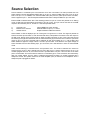
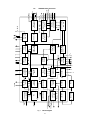
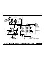
TDA884X Video Processor
Pin Designation I/O Description
1 SNDIF I Sound IF
2 AUDIOEXT I External Audio
3 NC Not Connected
4 NC Not Connected
5 PLLLF IF-PLL loop filter
6 IFVO O IF Video
7 SCL I Serial Clock
8 SDA I/O Serial data
9 DEC
BG
Bandgap de-coupling
10 CHROMA I Chrominance
11 CVBS/Y I External CVBS/Y
12 V
P1
Main supply voltage 1 (+8V)
13 CVBS
INT
I Internal CVBS
14 GND 1 Ground 1
15 AUDIOOUT O Audio
16 SECPLL SECAM PLL de-coupling
17 CVBS
EXT
I External CVBS
18 BLKIN I Black-current
19 BO O Blue
20 GO O Green
21 RO O Red
22 BCLIN I Beam current limiter input/V-guard input
23 RI I Red input for insertion
24 GI I Green input for insertion
25 BI I Blue input for insertion
27 RGBIN I RGB insertion
27 LUMIN I Luminance
28 LUMOUT O Luminance
29 BYO O (B-Y) signal
30 RYO O (R-Y) signal
31 BYI I (B-Y) signal
32 RYI I (R-Y) signal
33 REFO O Sub-carrier reference
34 XTAL1 3.58MHz crystal connection
35 XTAL2 4.43/3.58MHz crystal connection
36 DET Loop filter phase detector
37 V
P2
2nd supply voltage 1 (+8V)
38 CVBS1O O CVBS-1
39 DECDIG De-coupling digital supply
40 HOUT O Horizontal
41 FBISO I/O Flyback input/sandcastle output
42 PH2LF Phase-2 filter
43 PH1LF Phase-1 filter
44 GND2 Ground 2
45 EWD O East-west drive
46 VDRB O Vertical drive B
47 VDRA O Vertical drive A
48 IFIN1 I IF input 1
49I FIN2 I IF input 2
50 EHTO I EHT overvoltage protection
51 VSC Vertical sawtooth capacitor
52 I
REF
I Reference current
53 DEC
AGC
AGC de-coupling capacitor
54 AGCOUT O Tuner AGC
55 AUDEEM Audio de-emphasis
56 DECSDEM De-coupling sound demodulator
Table 2 – TDA884X
Pin Designations

19
9.2 TDA884X Video Processor
Fig 7
Block Diagram
AGC FOR IF
+ TUNER
SYNC SEP.
+ 1st LOOP
VCO
+ CONTROL
VIDEO
AMPLIFIER
VERT. SYNC.
SEPARATOR
VIDEO MUTE
FILTER
TUNING
2nd LOOP
HOR. OUT
H/V DIVIDER
CONTINUOUS
CATHODE
CALIBRATION
PRE-AMP.
+ MUTE
LUMA DELAY
PEAKING
CORING
PLL DEMOD.
CONTROL
DAC’s
CHROMA
TRAP
+ BANDPASS
CVBS-Y/C
SWITCH
CVBS SWITCH
PAL/NTSC
SECAM
DECODER
BASE-BAND
DELAY TIME
VERTICAL
GEOMETRY
RGB CONTROL
BLUE STRETCH
OUTPUT
BLACK
STRETCH
RGB MATRIX
RGB 1 INPUT
CD MATRIX
SAT. CONTROL
SKIN TINT
VIF AMPLIFIER
+ PLL DEMOD
+ CALIBRATION
AFC
VIDEO IDENT
AVL +
SWITCH +
VOLUME
LIMITER
SOUND
BANDPASS
SOUND
TRAP
48
49
IF-IN
53
8
7
54
5
15
55
45
56
10 11
35
3316343638 113
6
SD
AA
SCL
H-DRIVE
TUNER
TOP
POL
AFC
SW
REF
HUE
SW
CVBS OUT
C
V
B
S
I
N
MUTE
IDENT
A
UDIO OUT
2
AUDIO IN
VOL SW
I²C BUS
TRANSCEIVE
R
C
h
r
C
V
B
S/
Y
40
41
42
39
37
12
9
44
14
43
BRI
WHITE P
CONTR
50 EHT
46
47 V. DRIVE
52
51
21 R
20 G
19 B
22 BEAM CUR
R
18 BLACK CUR
R
23 R1
24 G1
25 G1
26 BL1
SAT
REF
F
SC

20
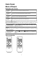
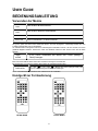
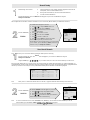
Remote Control
The remote control system used is the Philip’s Enhanced RC5 protocol, with sub-address 00000.
Infra-red Transmitter
The hand unit is controlled by IC781, type PCA84C122AT/093, surface mounted on the keypad side of the
PCB. When replacing the part, the /093 is significant as it determines the key codes transmitted. Two AA
type batteries in series provide a 3V power supply.
The IC remains in standby mode (oscillator not running) until a key on the matrix is pressed. The oscillator,
governed by a 4MHz ceramic resonator XL781 is started. The IC decodes the key with suitable debounce
and then transmits the relevant code, repeating as per the RC5 specification until the key is released.
The RC5 pulse train output is modulated within the IC onto a 33.33kHz (f.osc/120) carrier with low (1:3)
hark:space ratio, reducing power consumption and allowing higher LED current. The output on pin 21 of
IC781 drives TR781 which provides high current pulses through infra-red transmitter diode D781. Reservoir
capacitor CE781 reduces momentary battery voltage drop which may otherwise affect the IC.
Infra-red Receiver
The chassis uses an integrated receiver, IC702, which provides a fully demodulated output to the
microcontroller through R703, pulled up by R702.
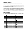
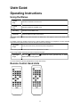
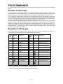
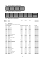
Keypad N° Symbol Functions Keypad N° Symbol Functions
1
! ."
Standby 16
#
Programme Up
2 1 N° 1 17
$"
Increase Volume
3 2 N° 2 18
%"
Decrease Volume
4 3 N° 3 19 *Fastext (RED)
5 4 N° 4 20 Menu/*Fastext (GREEN)
6 5 N° 5 21 Menu/*Fastext YELLOW)
7 6 N° 6 22 Menu/*Fastext (CYAN)
8 7 N° 7 23
&
"
Normalize/*Hold
9 8 N° 8 24
'
"
*Expand
10 9 N° 9 25
(
"
*Reveal
11 0 N° 0 26
)
))
)
""
Status/*Fastext Index
12
*
"
TV 27
+"
AV Select
13
,
"
*Text/*Mix 28
-
*Time/*Subcode
14
."
Programme Down 29
/
"
**Audio Select
15
0
"
Mute 30
1
"
*Update
* These functions are only present on chassis fitted with teletext
** These functions are only present on chassis fitted with stereo
Table 3
Keypad Idents and Functions
La page est en cours de chargement...
La page est en cours de chargement...
La page est en cours de chargement...
La page est en cours de chargement...
La page est en cours de chargement...
La page est en cours de chargement...
La page est en cours de chargement...
La page est en cours de chargement...
La page est en cours de chargement...
La page est en cours de chargement...
La page est en cours de chargement...
La page est en cours de chargement...
La page est en cours de chargement...
La page est en cours de chargement...
La page est en cours de chargement...
La page est en cours de chargement...
La page est en cours de chargement...
La page est en cours de chargement...
La page est en cours de chargement...
La page est en cours de chargement...
La page est en cours de chargement...
La page est en cours de chargement...
La page est en cours de chargement...
La page est en cours de chargement...
La page est en cours de chargement...
La page est en cours de chargement...
La page est en cours de chargement...
La page est en cours de chargement...
La page est en cours de chargement...
La page est en cours de chargement...
La page est en cours de chargement...
La page est en cours de chargement...
La page est en cours de chargement...
La page est en cours de chargement...
La page est en cours de chargement...
La page est en cours de chargement...
La page est en cours de chargement...
La page est en cours de chargement...
La page est en cours de chargement...
La page est en cours de chargement...
La page est en cours de chargement...
La page est en cours de chargement...
La page est en cours de chargement...
La page est en cours de chargement...
La page est en cours de chargement...
La page est en cours de chargement...
La page est en cours de chargement...
La page est en cours de chargement...
La page est en cours de chargement...
La page est en cours de chargement...
La page est en cours de chargement...
La page est en cours de chargement...
La page est en cours de chargement...
La page est en cours de chargement...
La page est en cours de chargement...
La page est en cours de chargement...
La page est en cours de chargement...
La page est en cours de chargement...
La page est en cours de chargement...
La page est en cours de chargement...
La page est en cours de chargement...
La page est en cours de chargement...
La page est en cours de chargement...
La page est en cours de chargement...
La page est en cours de chargement...
La page est en cours de chargement...
La page est en cours de chargement...
La page est en cours de chargement...
La page est en cours de chargement...
La page est en cours de chargement...
La page est en cours de chargement...
La page est en cours de chargement...
La page est en cours de chargement...
La page est en cours de chargement...
La page est en cours de chargement...
La page est en cours de chargement...
La page est en cours de chargement...
La page est en cours de chargement...
La page est en cours de chargement...
La page est en cours de chargement...
La page est en cours de chargement...
La page est en cours de chargement...
La page est en cours de chargement...
La page est en cours de chargement...
La page est en cours de chargement...
La page est en cours de chargement...
La page est en cours de chargement...
La page est en cours de chargement...
La page est en cours de chargement...
La page est en cours de chargement...
La page est en cours de chargement...
La page est en cours de chargement...
La page est en cours de chargement...
La page est en cours de chargement...
La page est en cours de chargement...
La page est en cours de chargement...
La page est en cours de chargement...
La page est en cours de chargement...
La page est en cours de chargement...
La page est en cours de chargement...
La page est en cours de chargement...
La page est en cours de chargement...
La page est en cours de chargement...
La page est en cours de chargement...
La page est en cours de chargement...
La page est en cours de chargement...
La page est en cours de chargement...
La page est en cours de chargement...
La page est en cours de chargement...
La page est en cours de chargement...
La page est en cours de chargement...
La page est en cours de chargement...
La page est en cours de chargement...
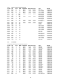
-
 1
1
-
 2
2
-
 3
3
-
 4
4
-
 5
5
-
 6
6
-
 7
7
-
 8
8
-
 9
9
-
 10
10
-
 11
11
-
 12
12
-
 13
13
-
 14
14
-
 15
15
-
 16
16
-
 17
17
-
 18
18
-
 19
19
-
 20
20
-
 21
21
-
 22
22
-
 23
23
-
 24
24
-
 25
25
-
 26
26
-
 27
27
-
 28
28
-
 29
29
-
 30
30
-
 31
31
-
 32
32
-
 33
33
-
 34
34
-
 35
35
-
 36
36
-
 37
37
-
 38
38
-
 39
39
-
 40
40
-
 41
41
-
 42
42
-
 43
43
-
 44
44
-
 45
45
-
 46
46
-
 47
47
-
 48
48
-
 49
49
-
 50
50
-
 51
51
-
 52
52
-
 53
53
-
 54
54
-
 55
55
-
 56
56
-
 57
57
-
 58
58
-
 59
59
-
 60
60
-
 61
61
-
 62
62
-
 63
63
-
 64
64
-
 65
65
-
 66
66
-
 67
67
-
 68
68
-
 69
69
-
 70
70
-
 71
71
-
 72
72
-
 73
73
-
 74
74
-
 75
75
-
 76
76
-
 77
77
-
 78
78
-
 79
79
-
 80
80
-
 81
81
-
 82
82
-
 83
83
-
 84
84
-
 85
85
-
 86
86
-
 87
87
-
 88
88
-
 89
89
-
 90
90
-
 91
91
-
 92
92
-
 93
93
-
 94
94
-
 95
95
-
 96
96
-
 97
97
-
 98
98
-
 99
99
-
 100
100
-
 101
101
-
 102
102
-
 103
103
-
 104
104
-
 105
105
-
 106
106
-
 107
107
-
 108
108
-
 109
109
-
 110
110
-
 111
111
-
 112
112
-
 113
113
-
 114
114
-
 115
115
-
 116
116
-
 117
117
-
 118
118
-
 119
119
-
 120
120
-
 121
121
-
 122
122
-
 123
123
-
 124
124
-
 125
125
-
 126
126
-
 127
127
-
 128
128
-
 129
129
-
 130
130
-
 131
131
-
 132
132
-
 133
133


Hitachi C1422R Manuel utilisateur
- Catégorie
- Téléviseurs LCD
- Taper
- Manuel utilisateur
dans d''autres langues
- English: Hitachi C1422R User manual
- Deutsch: Hitachi C1422R Benutzerhandbuch
Documents connexes
Autres documents
-
Armacost Lighting 714421 Mode d'emploi
-
Kenwood LSK 300 Le manuel du propriétaire
-
 JB DV-22N Digital Vacuum Gauge Manuel utilisateur
-
Premier ctv-2641sr Manuel utilisateur
-
Omega CLH-II Le manuel du propriétaire
-
AEG 191215 Alfie LED Ceiling Spotlight Manuel utilisateur
-
AEG 191213 LED Wall Spot Metal-Plastic Dimmable Mode d'emploi
-
HP Latex 3000 Printer Mode d'emploi
-
Grundig CUC 7301F Manuel utilisateur
-
