
YL430132
IEEE 802.11 a/b/g/n Wireless LAN and Bluetooth Combo Stamp Module
1. General Description
The YL430132 IEEE 802.11 a/b/g/n SDIO Wi-Fi with Bluetooth 5.0 combo
stamp module is a highly integrated wireless local area network (WLAN)
solution to let users enjoy the digital content through the latest wireless
technology without using the extra cables and cords. It combines with Bluetooth
5.0 and provides a complete 2.4GHz Bluetooth system which is fully compliant
to Bluetooth 5.0 with integrated PA for Class 1.5 and Low Energy (BLE) that
supports EDR of 2Mbps and 3Mbps for data and audio communications. It
enables a high performance, cost effective, low power, compact solution that
easily fits onto the SDIO and UART stamp module.
Compliant with the IEEE 802.11a/b/g/n standard, YL430132 uses Direct
Sequence Spread Spectrum (DSSS), Orthogonal Frequency Division
Multiplexing (OFDM), BPSK, QPSK, CCK and QAM baseband modulation
technologies.
A high level of integration and full implementation of the power management
functions specified in the IEEE 802.11 standard minimize system power
requirements by using YL430132.
YL430132 module adopts BCM430132 single chip solution. The module design
is based on the BCM430132 solution.
2. Key Features
1. Single spatial stream up to a 72 Mbps data rate.
2. 1(Transmit) ×1(Receive) Wi-Fi and Bluetooth 5.0
3. Low power consumption and high performance
4. Enhanced wireless security
5. Supports Bluetooth 5.0-compliant features
6. BDR、EDR(2、3Mbps)、LE(1Mbps) supported
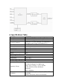
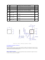
3. Block Diagram
A simplified block diagram of the YL430132 module is depicted in the figure below.

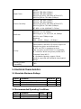
4. Specifications Table
Model Name
YL430132
Description
Wireless LAN &Bluetooth Stamp Module
WLAN Standard
IEEE 802.11a/b/g/n & Wi-Fi compliant
Bluetooth Standard
Bluetooth 2.1 + EDR, Bluetooth 3.0, Bluetooth 4.2
(Bluetooth Low Energy), and Bluetooth 5.0.
Major Chipset
BCM430132
Host Interface
Wi-Fi: SDIO, BT: UART
Dimensions
12mm * 12mm * 2.0mm
Wi-Fi VID/PID
TBD
BT VID/PID
TBD
Weight
TBD
Operating Conditions
Voltage
power supply for host:3.3V
Temperature
-40℃~85℃
Storage temperature
-45℃~135℃
Electrical Specifications
Frequency Range
WLAN:
2.4 GHz ISM Bands 2.4-2.4835 GHz
5Ghz: 5.15~5.35GHz、5.47~5.725GHz、
5.725~5.85GHz (5GHz UNII Band)
Bluetooth:
2402~2480MHz
Modulation
CCK、OFDM /64-QAM、16-QAM、QPSK、BPSK
for WLAN
GFSK, π/4-DQPSK, 8DPSK for Bluetooth

Output Power
WLAN:
802.11b: TBD dBm (11Mbps)
802.11g: TBD dBm (54Mbps)
802.11n @2.4GHz: TBD dBm (HT20 MCS7)
802.11a @5GHz: TBD dBm (54Mbps)
Receive Sensitivity
802.11b: TBD dBm (11Mbps)
802.11g: TBD dBm (54Mbps)
802.11n @2.4GHz: TBD dBm (HT20 MCS7)
802.11a @5GHz: TBD dBm (54Mbps)
BT: BER < 0.1% (IQXEL80 Tx -70 Bm)
Data Rates
WLAN
802.11b: 1, 2, 5.5, 11Mbps
802.11a/g: 6, 9, 12, 18, 24, 36, 48, 54Mbps
802.11n: up to 72Mbps-single
Bluetooth
BDR、EDR(2、3Mbps)、LE(1Mbps)
Security
◆WPA, WPA2 (Personal) with security
improvements, and WPA3 (Personal) support for
powerful encryption and authentication
◆AES and TKIP in hardware for faster
data encryption and IEEE 802.11i compatibility
◆Reference WLAN subsystem provides Wi-Fi
Protected Setup (WPS)
◆Worldwide regulatory support: Global
products supported with worldwide homologated
design
Operating System
Compatibility
TBD
5. Electrical Characteristics
5.1 Absolute Maximum Ratings
Symbol
Parameter
Maximum
Unit
VDD
3.3V power supply voltage
5.25
V
VDDIO
Voltage supply for GPIO
2.07
V
RFin
Maximum RF input (reference to 50 Ω)
TBD
dBm
5.2 Recommended Operating Conditions
Symbol
Parameter
Rating
Unit
VDD
3.3V power supply voltage
3.2~5.0
V
VDDIO
Voltage supply for GPIO
1.62~1.98
V

5.4 GPIO DC Characteristics
Symbol
Parameter
Minimum
Typical
Maximum
Unit
VIH
Input high voltage
0.65*VDDIO
--
VIO+0.3
V
VIL
Input low voltage
-0.3
--
0.35*0.65*VDDIO
V
VOH
Output high voltage
VDDIO-0.45
--
VIO
V
VOL
Output low voltage
0
--
0.45
V
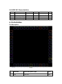
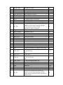
6. Pin Definition
Pin Description
Pin
No.
Definition
Basic Description Type
Type
1
GND
GROUND
GND

2
WL_BT_ANT
Wi-Fi/BT RF signal
I/O
3
GND
GROUND
GND
4
NC
Floating Pin, No connect to anything.
Floating
5
NC
Floating Pin, No connect to anything.
Floating
6
Host_Wakeup_BT
Host wakeup BT device
IN
7
BT_wakeup_Host
BT Device wakeup Host
I/O
8
NC/TMS
Reserve for EJTAG
I/O
9
VBAT
DC power supply +3.3V input
VCC
10
XTAL_IN/NC
Floating Pin, No connect to anything.
Floating
11
XTAL_OUT/NC
Floating Pin, No connect to anything.
Floating
12
WL_EN
GPIO pin to on/off the Wi-Fi function by
software. Active high. Reserve pull high
100K resistor and shunt 100pF
capacitor to GND on platform.
IN
13
WL_wakeup_Host
WLAN device wakeup host
OUT
14
SDIO_DATA2
SDIO Data Line 2
I/O
15
SDIO_DATA3
SDIO Data Line 3
I/O
16
SDIO_CMD
SDIO Command Input
I/O
17
SDIO_CLK
SDIO Clock Input
IN
18
SDIO_DATA0
SDIO Data Line 0
I/O
19
SDIO_DATA1
SDIO Data Line 1
I/O
20
GND
GROUND
GND
21
NC
Floating Pin, No connect to anything.
Floating
22
VDDIO
1.8V-3.3V VDDIO supply for WLAN and BT
VCC
23
NC
Floating Pin, No connect to anything.
Floating
24
LPO
External low-power 32.768KHz clock input.
IN
25
PCM_OUT
PCM synchronous data output, connected to
PCM_IN on the
host.
OUT
26
PCM_CLK
PCM Clock
I/O
27
PCM_IN
PCM synchronous data input, connected to
PCM_OUT on the
host.
IN
28
PCM_SYNC
PCM synchronous data SYNC
I/O
29
TDI
Reserve for EJTAG
IN
30
TDO
Reserve for EJTAG
OUT
31
GND
GROUND
GND
32
TCK
Reserve for EJTAG
GND
33
GND
GROUND
GND
34
BT_EN
GPIO pin to on/off the BT function by
software. Active high. Reserve pull high
100K resistor and shunt 100pF capacitor to
GND on host.
IN

35
NC
Floating Pin, No connect to anything.
Floating
36
GND
GROUND
GND
37
NC
Floating Pin, No connect to anything.
Floating
38
NC
Floating Pin, No connect to anything.
Floating
39
NC
Floating Pin, No connect to anything.
Floating
40
NC
Floating Pin, No connect to anything.
Floating
41
UART_RTS
UART Ready To Send, connected to CTS on
the host.
OUT
42
UART_TXD
UART Transmit Data, connected to RXD on
the host.
OUT
43
UART_RXD
UART Receive Data, connected to TXD on
the host.
IN
44
UART_CTS
UART Clear To Send, connected to RTS on
the host.
IN
FCC regulatory compliance statement
§15.19 Statement
This device complies with Part 15 of the FCC Rules. Operation is subject to the following two conditions: (1) this
device may not cause harmful interference, and (2) this device must accept any interference received, including
interference that may cause undesired operation.
§15.21 Information to user
Warning: changes or modifications not expressly approved by the party responsible for compliance could void
the user’s authority to operate the equipment.

⚫List of applicable FCC rules:
47 CFR Part 15, Subpart C 15.247
47 CFR Part 15, Subpart E 15.407
⚫Summarize the specific operational use conditions
The module can be used in teleconference machine. After installing this module, the telephone can be connected
to the router through a wireless network. In WIFI coverage, users can send various instructions through smart
phones or PCs, which is very convenient. The input voltage of the module is nominally 5V, and other antennas of
the same type with less than the original gain can be replaced.
⚫Limited module procedures
This module is a limited module.
⚫Trace antenna designs
The antenna is not a trace antenna.
⚫RF exposure considerations
This Module complies with FCC radiation exposure limits set forth for an uncontrolled environment. This
equipment should be installed and operated with a minimum distance of 20cm between the radiator and your
body. This transmitter must not be co-located or operating in conjunction with any other antenna or transmitter.
⚫Antennas
The module itself does not have an antenna. During the test, the host provides a PCB antenna with a maximum
gain of 3dBi.
If you desire to increase antenna gain and either change antenna type or use same antenna type certified, a Class
II permissive change application is required to be filed by us, or you (host manufacturer) can take responsibility
through the change in FCC ID (new application) procedure followed by a Class II permissive change application.
⚫Label and compliance information
Please notice that if the FCC identification number is not visible when the module is installed inside another
device, then the outside of the device into which the module is installed must also display a label referring to the
enclosed module. This exterior label can use wording such as the following: “Contains FCC ID: T2C-YL430132” any
similar wording that expresses the same meaning may be used.
§ 15.19 Labelling requirements shall be complied on end user device.
Labelling rules for special device, please refer to §2.925, § 15.19 (a)(5) and relevant KDB publications. For E-label,
please refer to §2.935.
⚫Information on test modes and additional testing requirements
Test software access to different test modes: Wifi Test Tool v1.4.0
Testing item, Frequencies, Transmit Power, Modulation Type, test Antennas can be selected on the test script
instructions.

⚫Additional testing, Part 15 Subpart B disclaimer
This modular transmitter is only FCC authorized for the specific rule parts listed on our grant, host product
manufacturer is responsible for compliance to any other FCC rules that apply to the host not covered by the
modular transmitter grant of certification.
Host manufacturer in any case shall ensure host product which is installed and operating with the module is in
compliant with Part 15B requirements.
Please note that For a Class B or Class A digital device or peripheral, the instructions furnished the user manual of
the end-user product shall include statement set out in §15.105 Information to the user or such similar statement
and place it in a prominent location in the text of host product manual. Original texts as following:
For Class B
Note: This equipment has been tested and found to comply with the limits for a Class B digital device, pursuant
to part 15 of the FCC Rules. These limits are designed to provide reasonable protection against harmful
interference in a residential installation. This equipment generates, uses and can radiate radio frequency
energy and, if not installed and used in accordance with the instructions, may cause harmful interference to
radio communications. However, there is no guarantee that interference will not occur in a particular
installation. If this equipment does cause harmful interference to radio or television reception, which can be
determined by turning the equipment off and on, the user is encouraged to try to correct the interference by
one or more of the following measures:
—Reorient or relocate the receiving antenna.
—Increase the separation between the equipment and receiver.
—Connect the equipment into an outlet on a circuit different from that to which the receiver is connected.
—Consult the dealer or an experienced radio/TV technician for help.
For Class A
Note: This equipment has been tested and found to comply with the limits for a Class A digital device, pursuant
to part 15 of the FCC Rules. These limits are designed to provide reasonable protection against harmful
interference when the equipment is operated in a commercial environment. This equipment generates, uses,
and can radiate radio frequency energy and, if not installed and used in accordance with the instruction
manual, may cause harmful interference to radio communications. Operation of this equipment in a residential
area is likely to cause harmful interference in which case the user will be required to correct the interference at
his own expense.
ISED compliance statement
This device contains licence-exempt transmitter(s)/receiver(s) that comply with Innovation, Science and
Economic Development Canada’s licence-exempt RSS(s). Operation is subject to the following two conditions:
(1) This device may not cause interference.
(2) This device must accept any interference, including interference that may cause undesired operation of the
device.

L’émetteur/récepteur exempt de licence contenu dans le présent appareil est conforme aux CNR d’Innovation,
Sciences et Développement économique Canada applicables aux appareils radio exempts de licence.
L’exploitation est autorisée aux deux conditions suivantes :
(1) L’appareil ne doit pas produire de brouillage;
(2) L’appareil doit accepter tout brouillage radioélectrique subi, même si le brouillage est susceptible d’en
compromettre le fonctionnement.
ISED Radiation Exposure statement
This equipment complies with IC RSS-102 radiation exposure limits set forth for an uncontrolled environment.
This equipment should be installed and operated with minimum distance 20cm between the radiator and your
body.
Cet équipement est conforme aux limites d'exposition aux radiations IC CNR-102 établies pour un environnement
non contrôlé. Cet équipement doit être installé et utilisé avec une distance minimale de 20cm entre le radiateur
et votre corps. Cet émetteur ne doit pas être colocalisé ou fonctionner en conjonction avec une autre antenne ou
un autre émetteur.
End Device Labelling
Please notice that if the IC identification number is not visible when the module is installed inside another device,
then the outside of the device into which the module is installed must also display a label referring to the
enclosed module. This exterior label can use wording such as the following: “Contains IC: 10741A-YL430132” any
similar wording that expresses the same meaning may be used.
L’étiquette d’homologation d’un module d’Innovation, Sciences et Développement économique Canada devra
être posée sur le produit hôte à un endroit bien en vue, en tout temps. En l’absence d’étiquette, le produit hôte
doit porter une étiquette sur laquelle figure le numéro d’homologation du module d’Innovation, Sciences et
Développement économique Canada, précédé du mot « contient », ou d’une formulation similaire allant dans le
même sens et qui va comme suit :
Contient IC: 10741A-YL430132 est le numéro d’homologation du module
5G Wi-Fi Use Notice
1. the device for operation in the band 5150-5250 MHz is only for indoor use to reduce the potential for
harmful interference to co-channel mobile satellite systems;
2. the maximum antenna gain permitted for devices in the bands 5250-5350 MHz and 5470-5725 MHz shall
comply with the e.i.r.p. limit; and
3. the maximum antenna gain permitted for devices in the band 5725-5825 MHz shall comply with the e.i.r.p.
limits specified for point-to-point and non point-to-point operation as appropriate.
4. Users should also be advised that high-power radars are allocated as primary users (i.e. priority users) of
the bands 5250-5350 MHz and 5650-5850 MHz and that these radars could cause interference and/or
damage to LE-LAN devices.
1. les dispositifs fonctionnant dans la bande 5150-5250 MHz sont réservés uniquement pour uneutilisation à
l’intérieur afin de réduire les risques de brouillage préjudiciable aux systèmes de satellites mobiles utilisant
les mêmes canaux;
2. le gain maximal d’antenne permis pour les dispositifs utilisant les bandes 5250-5350 MHz et5470-5725 MHz

doit se conformer à la limite de p.i.r.e.;
3. le gain maximal d’antenne permis (pour les dispositifs utilisant la bande 5725-5825 MHz) doit se conformer
à la limite de p.i.r.e. spécifiée pour l’exploitation point à point et non point à point, selon le cas.
4. De plus, les utilisateurs devraient aussi être avisés que les utilisateurs de radars de haute puissancesont
désignés utilisateurs principaux (c.-à-d., qu’ils ont la priorité) pour les bandes 5250-5350 MHz et 5650-5850
MHz et que ces radars pourraient causer du brouillage et/ou des dommages aux dispositifs LAN-EL.
This radio transmitter [IC: 10741A-YL430132] has been approved by Innovation, Science and Economic
Development Canada to operate with the antenna types listed below, with the maximum permissible gain
indicated. Antenna types not included in this list that have a gain greater than the maximum gain indicated for
any type listed are strictly prohibited for use with this device.
a list of all antenna types
PCB Antenna
3dBi
-
 1
1
-
 2
2
-
 3
3
-
 4
4
-
 5
5
-
 6
6
-
 7
7
-
 8
8
-
 9
9
-
 10
10


dans d''autres langues
- English: Yealink YL430132 User manual
Autres documents
-
AMOSENSE ASUNBM00 Manuel utilisateur
-
GREE GRJWB05-J Manuel utilisateur
-
Honeywell HWB11AC-PRT WiFi and BT Module Manuel utilisateur
-
MICROCHIP WBZ351 Manuel utilisateur
-
Eurotech ReliaGATE 10-14 Le manuel du propriétaire
-
-
Honda E4000-01 V-Twin Diesel Generator Manuel utilisateur
-
 LITE ON QCS403YA Manuel utilisateur
-
 Espressif ESP32-S3-MINI-1 Manuel utilisateur
-
GREE GRJWB05-J2 Manuel utilisateur

