


SPECIFICATIONS SUBJECT TO CHANGE WITHOUT NOTICE
Notice
While reasonable efforts have been made to assure the accuracy of this document, Telit assumes
no liability resulting from any inaccuracies or omissions in this document, or from use of the
information obtained herein. The information in this document has been carefully checked and is
believed to be entirely reliable. However, no responsibility is assumed for inaccuracies or
omissions. Telit reserves the right to make changes to any products described herein and
reserves the right to revise this document and to make changes from time to time in content
hereof with no obligation to notify any person of revisions or changes. Telit does not assume
any liability arising out of the application or use of any product, software, or circuit described
herein; neither does it convey license under its patent rights or the rights of others.
It is possible that this publication may contain references to, or information about Telit products
(machines and programs), programming, or services that are not announced in your country.
Such references or information must not be construed to mean that Telit intends to announce
such Telit products, programming, or services in your country.
Copyrights
This instruction manual and the Telit products described in this instruction manual may be,
include or describe copyrighted Telit material, such as computer programs stored in
semiconductor memories or other media. Laws in the Italy and other countries preserve for Telit
and its licensors certain exclusive rights for copyrighted material, including the exclusive right
to copy, reproduce in any form, distribute and make derivative works of the copyrighted
material. Accordingly, any copyrighted material of Telit and its licensors contained herein or in
the Telit products described in this instruction manual may not be copied, reproduced,
distributed, merged or modified in any manner without the express written permission of Telit.
Furthermore, the purchase of Telit products shall not be deemed to grant either directly or by
implication, estoppel, or otherwise, any license under the copyrights, patents or patent
applications of Telit, as arises by operation of law in the sale of a product.
Computer Software Copyrights
The Telit and 3rd Party supplied Software (SW) products described in this instruction manual
may include copyrighted Telit and other 3rd Party supplied computer programs stored in
semiconductor memories or other media. Laws in the Italy and other countries preserve for Telit
and other 3rd Party supplied SW certain exclusive rights for copyrighted computer programs,
including the exclusive right to copy or reproduce in any form the copyrighted computer
program. Accordingly, any copyrighted Telit or other 3rd Party supplied SW computer programs
contained in the Telit products described in this instruction manual may not be copied (reverse
engineered) or reproduced in any manner without the express written permission of Telit or the
3rd Party SW supplier. Furthermore, the purchase of Telit products shall not be deemed to grant
either directly or by implication, estoppel, or otherwise, any license under the copyrights,
patents or patent applications of Telit or other 3rd Party supplied SW, except for the normal
non-exclusive, royalty free license to use that arises by operation of law in the sale of a product.

Usage and Disclosure Restrictions
License Agreements
The software described in this document is the property of Telit and its licensors. It is furnished
by express license agreement only and may be used only in accordance with the terms of such
an agreement.
Copyrighted Materials
Software and documentation are copyrighted materials. Making unauthorized copies is
prohibited by law. No part of the software or documentation may be reproduced, transmitted,
transcribed, stored in a retrieval system, or translated into any language or computer language,
in any form or by any means, without prior written permission of Telit
High Risk Materials
Components, units, or third-party products used in the product described herein are NOT fault-
tolerant and are NOT designed, manufactured, or intended for use as on-line control equipment
in the following hazardous environments requiring fail-safe controls: the operation of Nuclear
Facilities, Aircraft Navigation or Aircraft Communication Systems, Air Traffic Control, Life
Support, or Weapons Systems (High Risk Activities"). Telit and its supplier(s) specifically
disclaim any expressed or implied warranty of fitness for such High Risk Activities.
Trademarks
TELIT and the Stylized T Logo are registered in Trademark Office. All other product or service
names are the property of their respective owners.
Copyright © Telit Communications S.p.A.

1. INTRODUCTION ........................................................................................................................................................... 7
1.1. SCOPE ....................................................................................................................................................................... 7
1.2. AUDIENCE ................................................................................................................................................................. 7
1.3. CONTACT INFORMATION, SUPPORT ........................................................................................................................... 7
1.4. TEXT CONVENTIONS ................................................................................................................................................. 8
1.5. RELATED DOCUMENTS ............................................................................................................................................. 8
2. OVERVIEW .................................................................................................................................................................... 9
3. XE910 MINI PCI EXPRESS CARD CONNECTIONS............................................................................................. 10
3.1. PIN-OUT ................................................................................................................................................................ 10
3.2. ANTENNA CONNECTORS ......................................................................................................................................... 12
4. POWER SUPPLY ......................................................................................................................................................... 13
4.1. POWER SUPPLY REQUIREMENTS ............................................................................................................................. 13
4.2. POWER CONSUMPTION ............................................................................................................................................ 14
5. GSM/WCDMA/LTE /CDMA RADIO SECTION ..................................................................................................... 15
5.1. XE910 MINI PCI PRODUCT VARIANTS .................................................................................................................... 15
5.2. TX AND RX CHARACTERISTICS ............................................................................................................................... 15
5.3. GSM/WCDMA/LTE/CDMA ANTENNA REQUIREMENTS ...................................................................................... 16
5.3.1. GSM/WCDMA/LTE/CDMA Antenna - Installation Guidelines ..................................................................... 18
5.4. ANTENNA DIVERSITY REQUIREMENTS .................................................................................................................... 19
5.5. GNSS RECEIVER ..................................................................................................................................................... 21
5.5.1. GNSS Performances ...................................................................................................................................... 21
5.5.2. GNSS RF Front End Design .......................................................................................................................... 21
6. LOGIC LEVEL SPECIFICATIONS .......................................................................................................................... 22
7. USB PORT ..................................................................................................................................................................... 22
7.1. USB 2.0 HS ............................................................................................................................................................ 22
8. SIM INTERFACE ........................................................................................................................................................ 23
9. CONTROL SIGNALS .................................................................................................................................................. 24
9.1. WAKE# .................................................................................................................................................................. 24
9.2. W_DISABLE# ....................................................................................................................................................... 26
9.3. LED_WWAN# ....................................................................................................................................................... 26
9.4. PERST# .................................................................................................................................................................. 27
10. AUDIO SECTION OVERVIEW ............................................................................................................................ 27
10.1. ELECTRICAL CHARACTERISTICS ............................................................................................................................. 28
10.2. CODEC EXAMPLE .................................................................................................................................................. 28
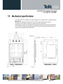
11. MECHANICAL SPECIFICATIONS ..................................................................................................................... 29
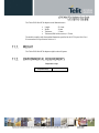
11.1. WEIGHT ................................................................................................................................................................ 30
11.2. ENVIRONMENTAL REQUIREMENTS .............................................................................................................. 30
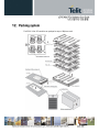
12. PACKING SYSTEM ................................................................................................................................................ 31
13. SAFETY RECOMMANDATIONS ......................................................................................................................... 32

14. CONFORMITY ASSESSMENT ISSUES .............................................................................................................. 33
1.1 1999/5/EC DIRECTIVE (HE910) ..................................................................................................................................... 33
14.1. FCC/IC REGULATORY NOTICES (HE910) ............................................................................................................... 36
1.2 1999/5/EC DIRECTIVE (LE910) ..................................................................................................................................... 38
14.2. FCC/IC REGULATORY NOTICES (LE910) ................................................................................................................ 41
14.3. CONFORMITY ASSESSMENT ISSUES / PROBLÈMES D'ÉVALUATION DE CONFORMITÉ (DE910) ................................. 44
14.4. SAFETY RECOMMENDATIONS (DE910) ................................................................................................................... 46
15. DOCUMENT HISTORY ......................................................................................................................................... 47

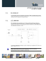
The aim of this document is the description of some hardware solutions useful for developing a
product with the Telit xE910 Mini PCIe Adapter.
This document is intended for Telit customers, who are integrators, about to implement their
applications using our xE910 Mini PCIe Adapter.
For general contact, technical support, to report documentation errors and to order manuals,
contact Telit’s Technical Support Center (TTSC) at:
TS-NORTHAMERI[email protected]
TS-LATINAMERI[email protected]
Alternatively, use:
http://www.telit.com/en/products/technical-support-center/contact.php
For detailed information about where you can buy the Telit modules or for recommendations on
accessories and components visit:
http://www.telit.com
To register for product news and announcements or for product questions contact Telit’s
Technical Support Center (TTSC).
Our aim is to make this guide as helpful as possible. Keep us informed of your comments and
suggestions for improvements.
Telit appreciates feedback from the users of our information.

Danger – This information MUST be followed or catastrophic equipment failure or bodily
injury may occur.
Caution or Warning – Alerts the user to important points about integrating the module, if
these points are not followed, the module and end user equipment may fail or malfunction.
Tip or Information – Provides advice and suggestions that may be useful when integrating
the module.
All dates are in ISO 8601 format, i.e. YYYY-MM-DD.
HE910/UE910 AT Commands Reference Guide 80378ST10091a
HE910 Hardware User Guide 1vv03700925
Event Monitor Application Note 80000nt10043a
Digital Voice Interface Application Note 80000NT10004a
LE910 AT Commands Reference Guide 80378ST10585a
LE910 Hardware User Guide 1vv03701089
LE910 Digital Voice Interface Application Note 80000NT11246a
DE910 Hardware User Guide 1vv03700951

The aim of this document is the description of some hardware solutions useful for developing a
product that will host the Telit XE910 Mini PCIe Adapter.
In this document all the basic functions of a mobile phone will be taken into account; for each
one of them a proper hardware solution will be suggested and eventually the wrong solutions
and common errors to be avoided will be evidenced. Obviously this document cannot embrace
the whole hardware solutions and products that may be designed. The wrong solutions to be
avoided shall be considered as mandatory, while the suggested hardware configurations shall not
be considered mandatory, instead the information given shall be used as a guide and a starting
point for properly developing your product with the Telit Mini PCIe module.
NOTICE:
(EN) The integration of the GSM/GPRS/WCDMA XE910 Mini PCIe cellular module within user
application shall be done according to the design rules described in this manual.
(IT) L’integrazione del modulo cellulare GSM/GPRS/WCDMA XE910 Mini PCIe all’interno
dell’applicazione dell’utente dovrà rispettare le indicazioni progettuali descritte in questo manuale.
(DE) Die Integration des XE910 Mini PCIe GSM/GPRS/WCDMA Mobilfunk-Moduls in ein Gerät muß
gemäß der in diesem Dokument beschriebenen Kunstruktionsregeln erfolgen.
(SL) Integracija GSM/GPRS/WCDMA XE910 Mini PCIe modula v uporabniški aplikaciji bo morala
upoštevati projektna navodila, opisana v tem priročniku.
(SP) La utilización del modulo GSM/GPRS/WCDMA XE910 Mini PCIe debe ser conforme a los usos
para los cuales ha sido deseñado descritos en este manual del usuario.
(FR) L’intégration du module cellulaire GSM/GPRS/WCDMA XE910 Mini PCIe dans l’application de
l’utilisateur sera faite selon les règles de conception décrites dans ce manuel.
(HE)
The information presented in this document is believed to be accurate and reliable. However, no
responsibility is assumed by Telit Communications S.p.A. for its use, nor any infringement of patents or
other rights of third parties which may result from its use. No license is granted by implication or
otherwise under any patent rights of Telit Communications S.p.A. other than for circuitry embodied in
Telit products. This document is subject to change without notice.
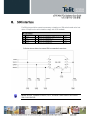
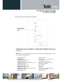
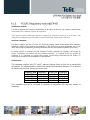
XE910 Mini PCIe

This product has a standard Mini PCI express connector, excepting the (4) audio signals which
use normally reserved connectors.
Pin
Signal
I/O
Function
Type
Power Supply
2
3V3_AUX
O
3.3V supply
Power
24
3V3
O
3.3V supply
Power
39
3V3_AUX
O
3.3V supply
Power
41
3V3_AUX
O
3.3V supply
Power
52
3V3_AUX
O
3.3V supply
Power
4
GND
-
Ground
Power
9
GND
-
Ground
Power
15
GND
-
Ground
Power
18
GND
-
Ground
Power
21
GND
-
Ground
Power
26
GND
-
Ground
Power
27
GND
-
Ground
Power
29
GND
-
Ground
Power
34
GND
-
Ground
Power
35
GND
-
Ground
Power
37
GND
-
Ground
Power
40
GND
-
Ground
Power
43
GND
-
Ground
Power
50
GND
-
Ground
Power
SIM Card Interface
8
SIMVCC
O
External SIM signal – Power supply for the SIM
1.8 / 3V
10
SIMIO
I/O
External SIM signal - Data I/O
1.8 / 3V
12
SIMCLK
O
External SIM signal – Clock
1.8 / 3V
14
SIMRST
O
External SIM signal – Reset
1.8 / 3V
USB
36
USB D-
I/O
USB differential Data (-)
0.3…2.8V
38
USB D+
I/O
USB differential Data (+)
0.3…2.8V

Pin
Signal
I/O
Function
Type
Miscellaneous Functions
1
WAKE#
O
Active low signal used to wake up the system from stand-by
3.3V
20
WDISABLE#
I
Active low signal for wireless disabling (Flight mode)
3.3V
22
PERST#
I
Active low functional reset to the card
3.3V
42
LED_WWAN#
O
Active low, open drain signal for WWAN LED driving, used to provide
module’s status indication
3.3V…5V
Digital Voice Interface (DVI)
45
PCM_CLK
I/O
Digital Audio Interface (CLK)
CMOS 1.8V
47
PCM_RX
I
Digital Audio Interface (RX)
CMOS 1.8V
49
PCM_TX
O
Digital Audio Interface (TX)
CMOS 1.8V
51
PCM_SYNC
I/O
Digital Audio Interface (SYNC)
CMOS 1.8V
N.C.
3
-
5
-
6
-
7
-
11
-
13
-
16
-
17
-
19
-
23
-
25
-
28
-
30
-
31
-
32
-
33
-
44
-
46
-
48
-

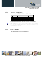
The xE910 Mini PCIe adapter is equipped with a set of 50 Ω RF U.FL. connectors from Hirose
U.FL-R-SMT-1(10).
The available connectors are:
Main RF antenna (ANT)
RX Diversity Antenna (DIV)
GNSS Antenna (GPS)
See the picture on the right for their position on the
interface.
The presence of all the connectors is depending on the
product characteristics and supported functionalities.
For more information about mating connectors, visit the website
http://www.hirose-connectors.com/

The power supply circuitry and board layout are a very important part in the full product design
and they strongly reflect on the product overall performances, hence read the requirements
carefully and the guidelines that will follow for a proper design.
The external power supply must be connected to the pins 2, 39, 41, 52 and must fulfill the
following requirements:
POWER SUPPLY
Nominal Supply Voltage
3.3 V
Normal Operating Voltage Range
3.00 V÷ 3.60 V
NOTE:
The Operating Voltage Range MUST never be exceeded; care must be taken when designing the
application’s power supply section to avoid having an excessive voltage drop.
If the voltage drop is exceeding the limits it could cause a Power Off of the module.
NOTE:
Overshoot voltage (regarding MAX Operating Voltage) and drop in voltage (regarding MIN
Operating Voltage) MUST never be exceeded;

Please refer to the Module’s Hardware User guide for the details
The GSM system is made in a way that the RF transmission is not continuous, else it is packed
into bursts at a base frequency of about 216 Hz, and the relative current peaks can be as high as
about 2.4A. Therefore the power supply has to be designed in order to withstand with these
current peaks without big voltage drops; this means that both the electrical design and the board
layout must be designed for this current flow. If the voltage drop during the peak current
absorption is too much, then the device may even shutdown as a consequence of the supply
voltage drop.
NOTE:
The electrical design for the Power supply should be made ensuring it will be capable of a peak
current output of at least 2.4 A.

The following table is listing the main differences between the xE910 variants:
Product
2G Bands
3G Bands
LTE Bands
CDMA Bands
GNSS
LE910-EUG
GSM 900,
DCS1800
B5(850), B8
(900), B1 (2100)
B20 (800), B3
(1800), B7 (2600)
NO
YES
LE910-NAG
GSM 850, PCS
1900
B5(850),
B2(1900)
B17(700), B5(850),
B4(1700), B2(1900)
NO
YES
LE910-NVG
Not supported
B5(850),
B2(1900)
B13(700), B4(1700)
NO
YES
LE910-SVG
Not supported
Not supported
B13(700), B4(1700)
NO
YES
HE910
GSM 850, GSM
900, DCS1800,
PCS 1900
FDD B1, B2, B4,
B5, B8
Not supported
NO
YES
HE910-D
GSM 850, GSM
900, DCS1800,
PCS 1900
FDD B1, B2, B4,
B5, B8
Not supported
NO
NO
DE910-
DUAL
Not supported
Not supported
Not supported
BC0, BC1
YES
Please refer to the Module’s Hardware User guide for the details

The antenna connection is one of the most important aspect in the full product design as it
strongly affects the product overall performances, hence read carefully and follow the
requirements and the guidelines for a proper design.
The xE910 Mini PCIe adapter is provided with three RF connectors.
The available connectors are:
Main RF antenna (ANT)
RX Diversity Antenna (DIV)
GNSS Antenna (GPS)
Connecting cables between the module and the antenna must have 50 Ω impedance.
If the impedance of the module is mismatched, RF performance is reduced significantly.
If the host device is not designed to use the module’s diversity or GPS antenna, terminate the
interface with a 50Ω load.
MAIN ANTENNA REQUIREMENTS for LE910-EUG
Frequency range
Depending by frequency band(s) provided by the network operator, the
customer shall use the most suitable antenna for that/those band(s)
Bandwidth (GSM/EDGE)
GSM900 : 80 MHz
GSM1800(DCS) : 170 MHz
Bandwidth
(WCDMA)
WCDMA band I(2100) : 250 MHz
WCDMA band V(850) : 70 MHz
WCDMA band VIII(900) : 80 MHz
Bandwidth
(LTE)
LTE band III(1800) : 170 MHz
LTE Band VII(2600) : 190 MHz
LTE Band XX(800) : 71 MHz
Impedance
50 ohm
Input power
> 33dBm(2 W) peak power in GSM
> 24dBm Average power in WCDMA & LTE
VSWR absolute max
≤ 10:1 (limit to avoid permanent damage)
VSWR recommended
≤ 2:1 (limit to fulfil all regulatory requirements)

MAIN ANTENNA REQUIREMENTS for LE910-NAG
Frequency range
Depending by frequency band(s) provided by the network operator, the
customer shall use the most suitable antenna for that/those band(s)
Bandwidth (GSM/EDGE)
GSM850 : 70 MHz
GSM1900(PCS) : 140 MHz
Bandwidth
(WCDMA)
WCDMA band II(1900) : 140 MHz
WCDMA band V(850) : 70 MHz
Bandwidth
(LTE)
LTE Band II(1900) : 140 MHz
LTE Band IV(1700) : 445 MHz
LTE Band V (850) : 70 MHz
LTE Band XVII(700) : 42 MHz
Impedance
50 ohm
Input power
> 33dBm(2 W) peak power in GSM
> 24dBm Average power in WCDMA & LTE
VSWR absolute max
≤ 10:1 (limit to avoid permanent damage)
VSWR recommended
≤ 2:1 (limit to fulfil all regulatory requirements)
MAIN ANTENNA REQUIREMENTS for LE910-NVG
Frequency range
Depending by frequency band(s) provided by the network operator, the
customer shall use the most suitable antenna for that/those band(s)
Bandwidth
(WCDMA)
WCDMA band II(1900) : 140 MHz
WCDMA band V(850) : 70 MHz
Bandwidth
(LTE)
LTE Band IV(1700) : 445 MHz
LTE Band XIII(700) : 41 MHz
Impedance
50 ohm
Input power
> 24dBm Average power in WCDMA & LTE
VSWR absolute max
≤ 10:1 (limit to avoid permanent damage)
VSWR recommended
≤ 2:1 (limit to fulfil all regulatory requirements)
MAIN ANTENNA REQUIREMENTS for LE910-SVG
Frequency range
Depending by frequency band(s) provided by the network operator, the
customer shall use the most suitable antenna for that/those band(s)
Bandwidth
(LTE)
LTE Band IV(1700) : 445 MHz
LTE Band XIII(700) : 41 MHz
Impedance
50 ohm
Input power
> 24dBm Average power
VSWR absolute max
≤ 10:1 (limit to avoid permanent damage)
VSWR recommended
≤ 2:1 (limit to fulfil all regulatory requirements)

MAIN ANTENNA REQUIREMENTS for HE910
Frequency range
Depending by frequency band(s) provided by the network operator, the
customer shall use the most suitable antenna for that/those band(s)
Bandwidth (GSM/EDGE)
70 MHz in GSM850, 80 MHz in GSM900, 170 MHz in DCS & 140 MHz
PCS band
Bandwidth
(WCDMA)
70 MHz in WCDMA Band V
80 MHz in WCDMA Band VIII
460 MHz in WCDMA Band IV
140 MHz in WCDMA Band II
250 MHz in WCDMA Band I
Impedance
50 ohm
Input power
> 33dBm(2 W) peak power in GSM
> 24dBm Average power in WCDMA
VSWR absolute max
≤ 10:1 (limit to avoid permanent damage)
VSWR recommended
≤ 2:1 (limit to fulfil all regulatory requirements)
MAIN ANTENNA REQUIREMENTS for DE910-DUAL
Frequency range
Depending by frequency band(s) provided by the network operator, the
customer shall use the most suitable antenna for that/those band(s)
Bandwidth
70 MHz in CDMA BC0
140 MHz in CDMA BC1
Gain
Gain < 5.12dBi in CDMA BC0
Gain < 6.12dBi in CDMA BC1
Impedance
50 ohm
Input power
> 24.4dBm Average Power in CDMA
VSWR absolute max
≤ 5:1 (Limit to avoid permanent damage)
VSWR recommended
≤ 2:1 (limit to fulfil all regulatory requirements)
Please refer to the Module’s Hardware User guide for the details
Install the antenna in a place covered by the GSM/WCDMA/LTE/CDMA signal.
If the device antenna is located greater then 20cm from the human body and there are no co-
located transmitters then the Telit FCC/IC approvals can be re-used by the end product
If the device antenna is located less than 20cm from the human body or there are no co-
located transmitters then the additional FCC/IC testing may be required for the end product
(Telit FCC/IC approvals cannot be reused)
Antenna shall not be installed inside metal cases
Antenna shall be installed also according antenna manufacturer instructions.

This product includes an input for a second RX antenna to improve the radio sensitivity.
The function is called Antenna Diversity.
DIVERSITY ANTENNA REQUIREMENTS for LE910-EUG
Frequency range
Depending by frequency band(s) provided by the network operator, the
customer shall use the most suitable antenna for that/those band(s)
Bandwidth
(WCDMA)
WCDMA band I(2100) : 250 MHz
WCDMA band V(850) : 70 MHz
WCDMA band VIII(900) : 80 MHz
Bandwidth
(LTE)
LTE band III(1800) : 170 MHz
LTE Band VII(2600) : 190 MHz
LTE Band XX(800) : 71 MHz
Impedance
50 ohm
VSWR recommended
≤ 2:1 (limit to fulfil all regulatory requirements)
DIVERSITY ANTENNA REQUIREMENTS for LE910-NAG
Frequency range
Depending by frequency band(s) provided by the network operator, the
customer shall use the most suitable antenna for that/those band(s)
Bandwidth
(WCDMA)
WCDMA band II(1900) : 140 MHz
WCDMA band V(850) : 70 MHz
Bandwidth
(LTE)
LTE Band II(1900) : 140 MHz
LTE Band IV(1700) : 445 MHz
LTE Band V (850) : 70 MHz
LTE Band XVII(700) : 42 MHz
Impedance
50 ohm
VSWR recommended
≤ 2:1 (limit to fulfil all regulatory requirements)
DIVERSITY ANTENNA REQUIREMENTS for LE910-NVG
Frequency range
Depending by frequency band(s) provided by the network operator, the
customer shall use the most suitable antenna for that/those band(s)
Bandwidth
(WCDMA)
WCDMA band II(1900) : 140 MHz
WCDMA band V(850) : 70 MHz
Bandwidth
(LTE)
LTE Band IV(1700) : 445 MHz
LTE Band XIII(700) : 41 MHz
Impedance
50 ohm
VSWR recommended
≤ 2:1 (limit to fulfil all regulatory requirements)

DIVERSITY ANTENNA REQUIREMENTS for LE910-SVG
Frequency range
Depending by frequency band(s) provided by the network operator, the
customer shall use the most suitable antenna for that/those band(s)
Bandwidth
(LTE)
LTE Band IV(1700) : 445 MHz
LTE Band XIII(700) : 41 MHz
Impedance
50 ohm
VSWR recommended
≤ 2:1 (limit to fulfil all regulatory requirements)
DIVERSITY ANTENNA REQUIREMENTS for HE910
Frequency range
Depending by frequency band(s) provided by the network operator, the
customer shall use the most suitable antenna for that/those band(s)
Bandwidth (GSM/EDGE)
70 MHz in GSM850, 80 MHz in GSM900 & 140 MHz PCS band
Bandwidth
(WCDMA)
70 MHz in WCDMA Band V
80 MHz in WCDMA Band VIII
140 MHz in WCDMA Band II
250 MHz in WCDMA Band I
Impedance
50 ohm
VSWR recommended
≤ 2:1 (limit to fulfil all regulatory requirements)
DIVERSITY ANTENNA REQUIREMENTS for DE910-DUAL
Frequency range
Depending by frequency band(s) provided by the network operator, the
customer shall use the most suitable antenna for that/those band(s)
Bandwidth
70 MHz in CDMA BC0
140 MHz in CDMA BC1
Impedance
50 ohm
VSWR recommended
≤ 2:1 (limit to fulfil all regulatory requirements)
The second Rx antenna should not be located in the close vicinity of main antenna. In order to
improve Diversity Gain, Isolation and reduce mutual interaction, the two antennas should be
located at the maximum reciprocal distance possible, taking into consideration the available
space in the application.
NOTE1:
On HE910 the diversity is not supported on the FDD BAND IV and DCS band.
NOTE2:
In case of HE910, if the RX Diversity is not used/connected, disable the Diversity functionality
using the AT#RXDIV command (ref to the At User guide for the proper syntax).
La page est en cours de chargement...
La page est en cours de chargement...
La page est en cours de chargement...
La page est en cours de chargement...
La page est en cours de chargement...
La page est en cours de chargement...
La page est en cours de chargement...
La page est en cours de chargement...
La page est en cours de chargement...
La page est en cours de chargement...
La page est en cours de chargement...
La page est en cours de chargement...
La page est en cours de chargement...
La page est en cours de chargement...
La page est en cours de chargement...
La page est en cours de chargement...
La page est en cours de chargement...
La page est en cours de chargement...
La page est en cours de chargement...
La page est en cours de chargement...
La page est en cours de chargement...
La page est en cours de chargement...
La page est en cours de chargement...
La page est en cours de chargement...
La page est en cours de chargement...
La page est en cours de chargement...
La page est en cours de chargement...
-
 1
1
-
 2
2
-
 3
3
-
 4
4
-
 5
5
-
 6
6
-
 7
7
-
 8
8
-
 9
9
-
 10
10
-
 11
11
-
 12
12
-
 13
13
-
 14
14
-
 15
15
-
 16
16
-
 17
17
-
 18
18
-
 19
19
-
 20
20
-
 21
21
-
 22
22
-
 23
23
-
 24
24
-
 25
25
-
 26
26
-
 27
27
-
 28
28
-
 29
29
-
 30
30
-
 31
31
-
 32
32
-
 33
33
-
 34
34
-
 35
35
-
 36
36
-
 37
37
-
 38
38
-
 39
39
-
 40
40
-
 41
41
-
 42
42
-
 43
43
-
 44
44
-
 45
45
-
 46
46
-
 47
47


Telit Wireless Solutions HE910-D Manuel utilisateur
- Taper
- Manuel utilisateur
- Ce manuel convient également à
dans d''autres langues
Documents connexes
Autres documents
-
Miniso P66 Manuel utilisateur
-
Disney 087-16-7728 Manuel utilisateur
-
 Miniso EBS-1005 Wireless Soundbar Manuel utilisateur
-
Eurotech DynaGATE 10-12 Le manuel du propriétaire
-
Trebs MT-060 Fiche technique
-
Eurotech ReliaGATE 10-12 Le manuel du propriétaire
-
AJAX 20279 Mode d'emploi
-
-
-
